Meaning
Thermoset polymeric packaging surrounding integrated circuits is selectively dissolved through controlled exposure to heated concentrated acids to expose underlying semiconductor dies, bond wires and substrate traces without inducing mechanical destruction. Known as chemical de-encapsulation, this destructive laboratory procedure provides direct optical, physical and electrical access to internal active silicon for root-cause failure evaluation and quality audits. The technique isolates silicon failure modes, wire sweep conditions, pad corrosion and micro-cracking across microcontrollers, radio frequency front ends and power management units.
The boundary of the process stops when aggressive acid chemistry attacks sensitive aluminum bond wires or copper metallization layers, which ruins delicate internal electrical circuits.
Etching Mechanism
Nitric and sulfuric acid blends operate at temperatures between sixty and ninety degrees Celsius to digest cross-linked epoxy novolac matrixes containing silica filler particles. The acid breaks polymer carbon chains into soluble organic fragments, which wash away along with loose silicate grain additives during solvent rinse cycles. Precise ratio adjustment prevents the acid mixture from attacking fragile internal copper wire bonds or substrate ball interconnects.
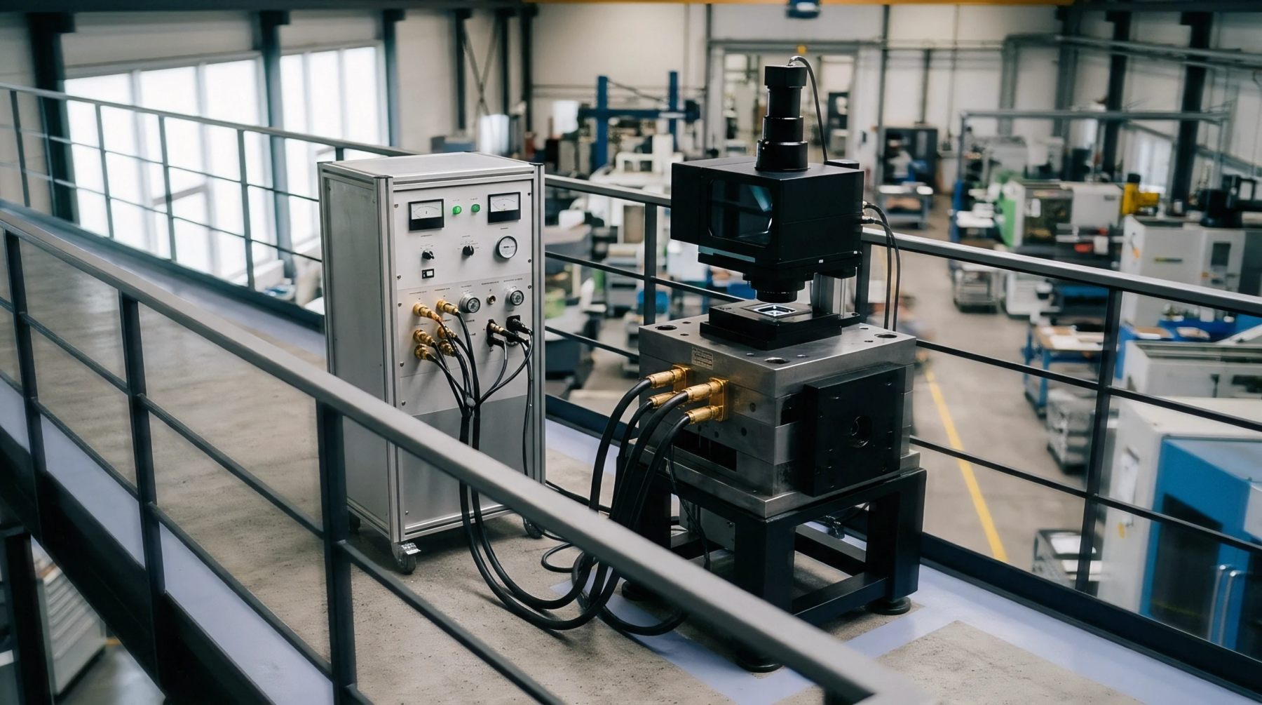
Automated jet etchers control acid volume, impingement velocity, temperature profiles and exposure windows to avoid collateral damage to internal die elements. Process completion leaves the internal silicon surface completely clear of organic residue.
Analytical Workflows
Laboratory technicians employ opened device cavities to execute micro-probing, scanning electron microscopy, energy-dispersive X-ray analysis, and photon emission microscopy. Wire bond integrity checks verify whether intermetallic phases between bonding wires and aluminum die pads comply with pull-force quality criteria. Internal layout verification detects unauthorized silicon alterations, wafer fab origin discrepancies, and silicon revision updates.
De-encapsulation work logs document etch parameters, acid chemistries and visual die health before engineering teams commit parts to electrical micro-probing.
Failure Identification
Exposed die surfaces display catastrophic overstress signatures such as gate oxide punch-through, metal trace electromigration, and electrostatic discharge burn sites that remain invisible through external non-destructive packaging inspections. Corrosion tracks caused by ionic ingress or moisture contamination across passivation layers appear clearly under scanning electron imaging. Counterfeit screening tracks silicon die part designations and copyright dates against package markings revealed before acid processing.
Test reports synthesize die imaging and electrical findings to assign structural fault attribution to either wafer fabrication errors or component mounting stress.