Meaning
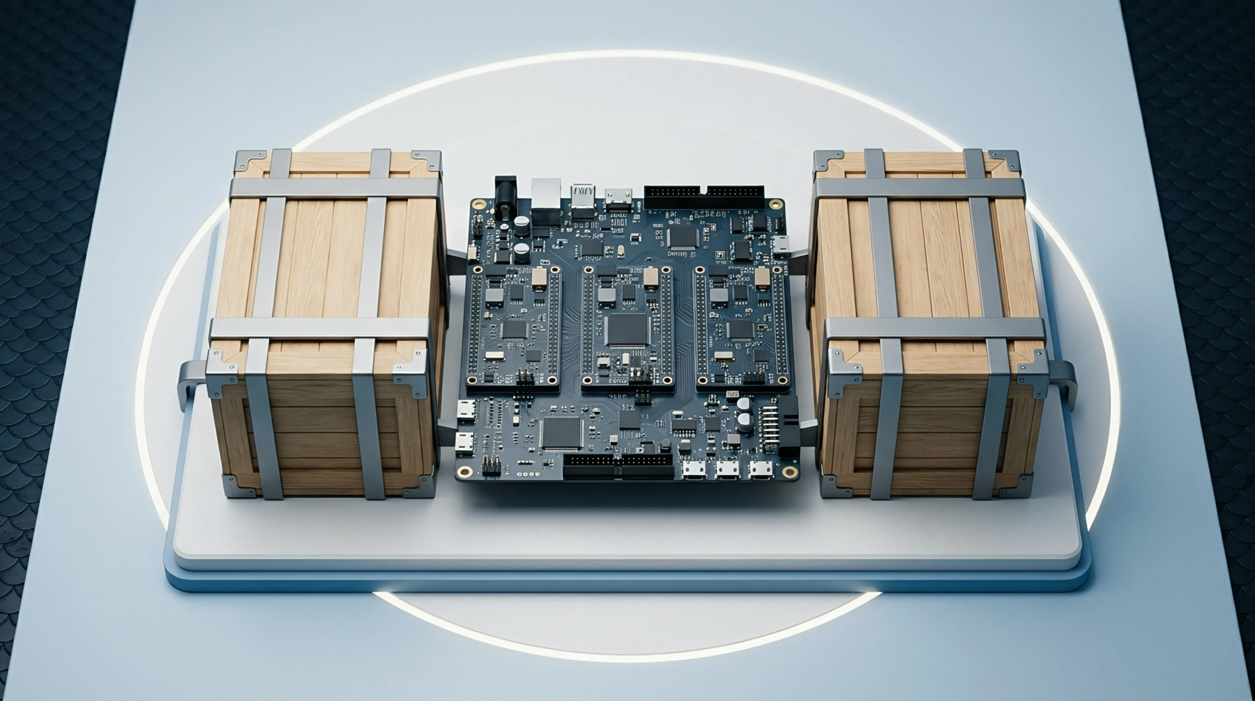
Vector image files formatted under the IEEE RS-274X or Gerber X3 specifications define two-dimensional copper traces, drill locations, solder masks and legend printing for printed circuit board fabrication. Manufacturing equipment interprets these geometric instructions to expose photoresist layers and guide automated optical inspection tools. Engineering teams export Gerber artwork from computer-aided design software as the final mechanical interface handover to board fabricators.
The scope of this file format stops at physical board layout geometry, excluding component bill of materials and circuit schematic netlists.
Production Handover
Fabrication houses extract aperture definitions and feature coordinates directly from geometry files to write photolithography tooling. Automated scripts verify trace clearance and annular ring width against factory capability matrices. Incomplete artwork generation results in exposed copper shorts or open trace faults during wet etching.
Quality Verification
Automated optical inspection scanners compare etched copper features directly against the original vector artwork file. Photolithography alignment marks ensure accurate registration between inner power planes and outer signal layers.
Layer Alignment
Differential pair skew and ground plane voiding depend on exact vector coordinates defined within physical layout files. Mechanical tolerances during film plotting can introduce overlay misregistration across large panel formats. Layout designers specify fiducial marks within Gerber artwork to anchor layer alignment during multi-layer lamination processes.