Meaning
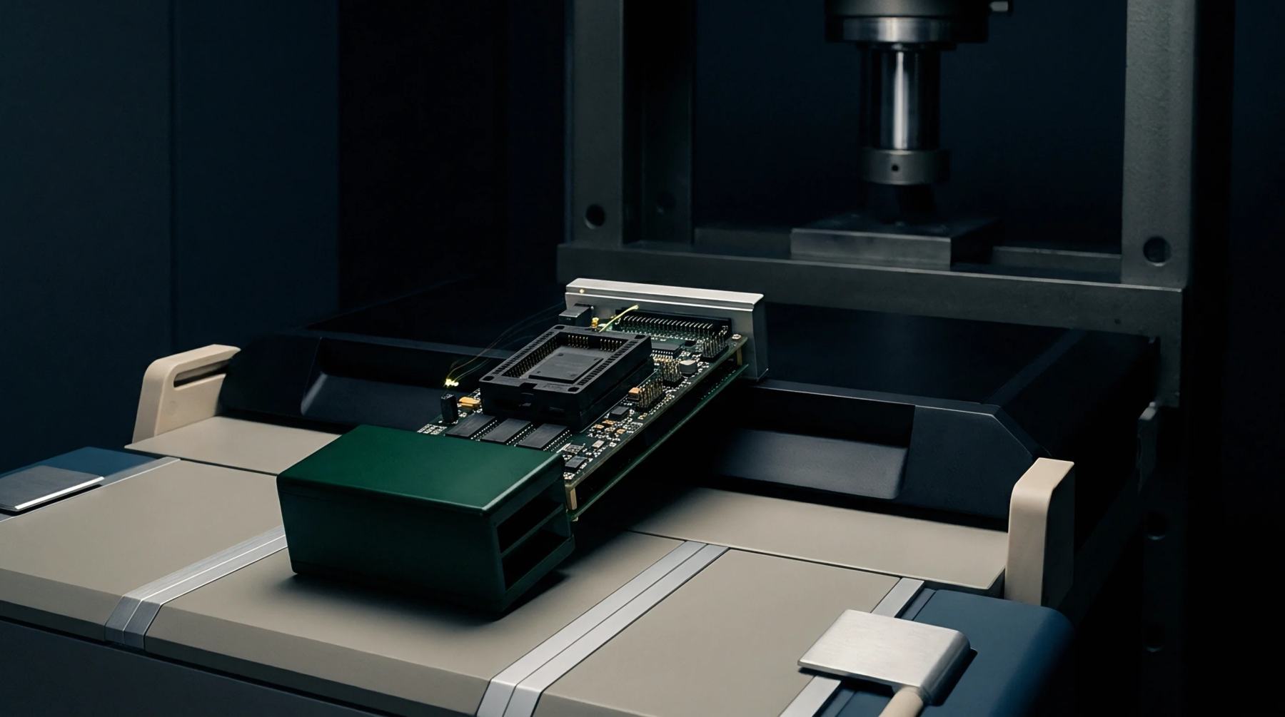
Physical configuration defines the spatial arrangement of sockets and connector interfaces on a hardware test platform. This loadboard layout optimizes electrical path lengths between a device under test and the automatic test equipment. Signal integrity depends upon the precise placement of bypass capacitors and ground planes within this grid.
Shortening the distance between pins reduces parasitic inductance which prevents oscillations during high frequency switching.
Mechanical Constraint
Thermal expansion creates misalignment risks for precision pogo pins. A loadboard layout accommodates these stresses by using slots or floating mounts rather than rigid fasteners. Material thickness must support the mass of the socket without bowing under pressure.
Designers select substrate types like polyimide or high glass transition temperature laminates to maintain dimensional stability.
Interface Topology
Routing density dictates the distribution of power and data lines across the board surface. Every loadboard layout separates sensitive analog signals from digital control lines to mitigate crosstalk. Isolation zones prevent noise injection from high speed data streams into precision measurement channels.
Vias are placed according to impedance matching requirements rather than component proximity alone.
Production Verification
Qualification protocols require a golden unit test to validate electrical performance across the entire interface. The loadboard layout undergoes rigorous inspection for solder joint defects and surface finish uniformity before the start of device production. Failure to adhere to the designated physical geometry results in intermittent contact or catastrophic signal loss at the wafer contact point.
Comprehensive verification of this interface ensures that measured performance data accurately reflects the underlying device characteristics.