Meaning
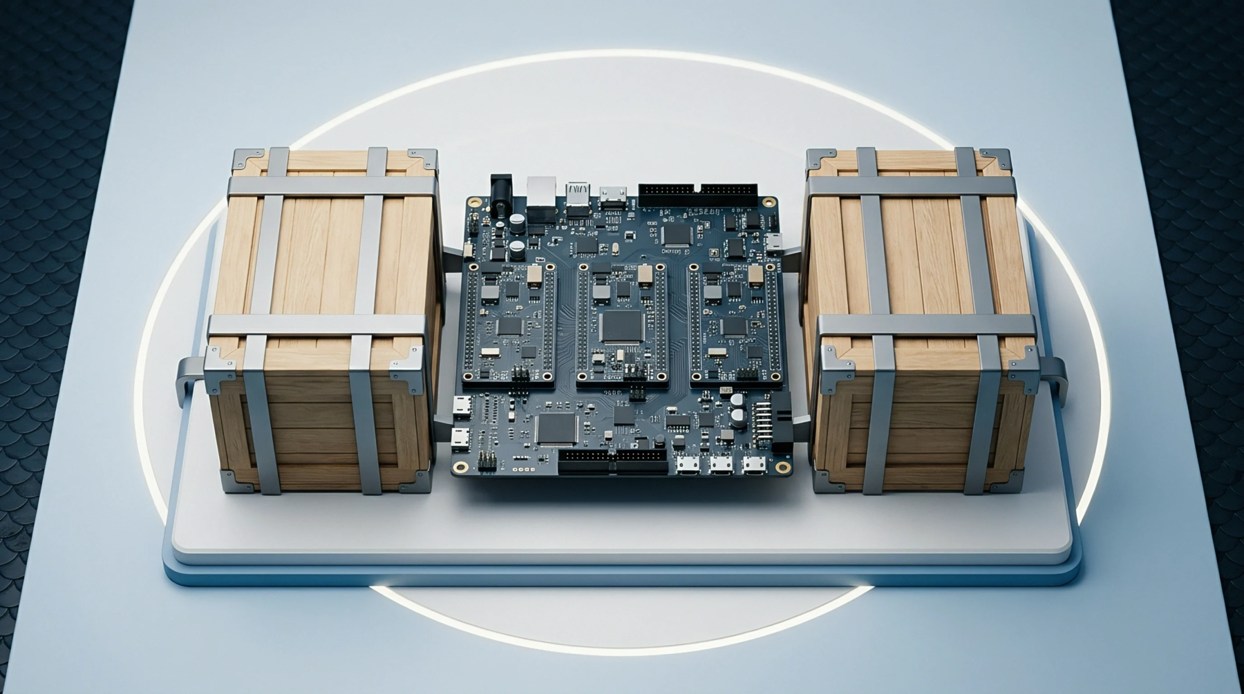
Semiconductor memory architecture permits real-time execution or data retrieval from one sector while simultaneous erase or program cycles operate on an alternate sector within the same component. The read while write capability separates internal memory array addressing and charge distribution logic, enabling uninterrupted instruction execution during active memory modifications. Microcontrollers and discrete flash memory devices implement this architecture to maintain time-critical task scheduling while writing persistent system parameters, audit logs, or incoming firmware images.
Memory contention boundaries apply strictly across distinct physical blocks, because reading from an active erasing block immediately triggers a hardware bus fault.
Bus Arbitration
Flash memories traditionally lock access buses during erase and program sequences because internal charge pumps must route high programming voltages across the silicon array. Devices with read while write capability isolate internal bus structures into distinct memory planes supported by dedicated charge generation circuitry. While a background programming cycle runs in a low-priority configuration storage sector, core processor instructions continue fetching from primary execution memory without memory pipeline stalls.
Cellular connectivity stacks and serial bus decoders operate without timing jitter during non-volatile write routines. Interrupt service routines execute instantly from internal flash, eliminating latency penalties caused by staging critical code in volatile static random access memory.
System Efficiency
Real-time embedded products reduce random access memory footprint requirements by relying on continuous memory access across firmware update operations. Telemetry devices store continuous sensor readings directly to non-volatile banks without freezing peripheral bus monitoring or network communication protocols. System architects eliminate external storage components by leveraging internal partitioned flash for both execution and data storage.
System reliability increases when microcontrollers maintain continuous operational control during prolonged multi-megabyte memory programming operations.
Integration Testing
Hardware validation protocols measure read bus response times during high-voltage write operations to ensure signal integrity across memory bank boundaries. Technicians configure automated oscilloscopes and logic analyzers to detect wait-state insertions or bus hold-offs while triggering background block erases during continuous direct memory access read streams. Qualification documents capture worst-case read access latencies under elevated ambient temperatures to verify that write pump noise does not induce bit errors across reading blocks.
Engineering sign-off requires uninterrupted pulse-width modulation output and zero dropped communications packets during sustained sector erase cycles on adjacent memory partitions. Bus fault handlers catch illegal simultaneous access commands directed to single-sector memory regions.