Meaning
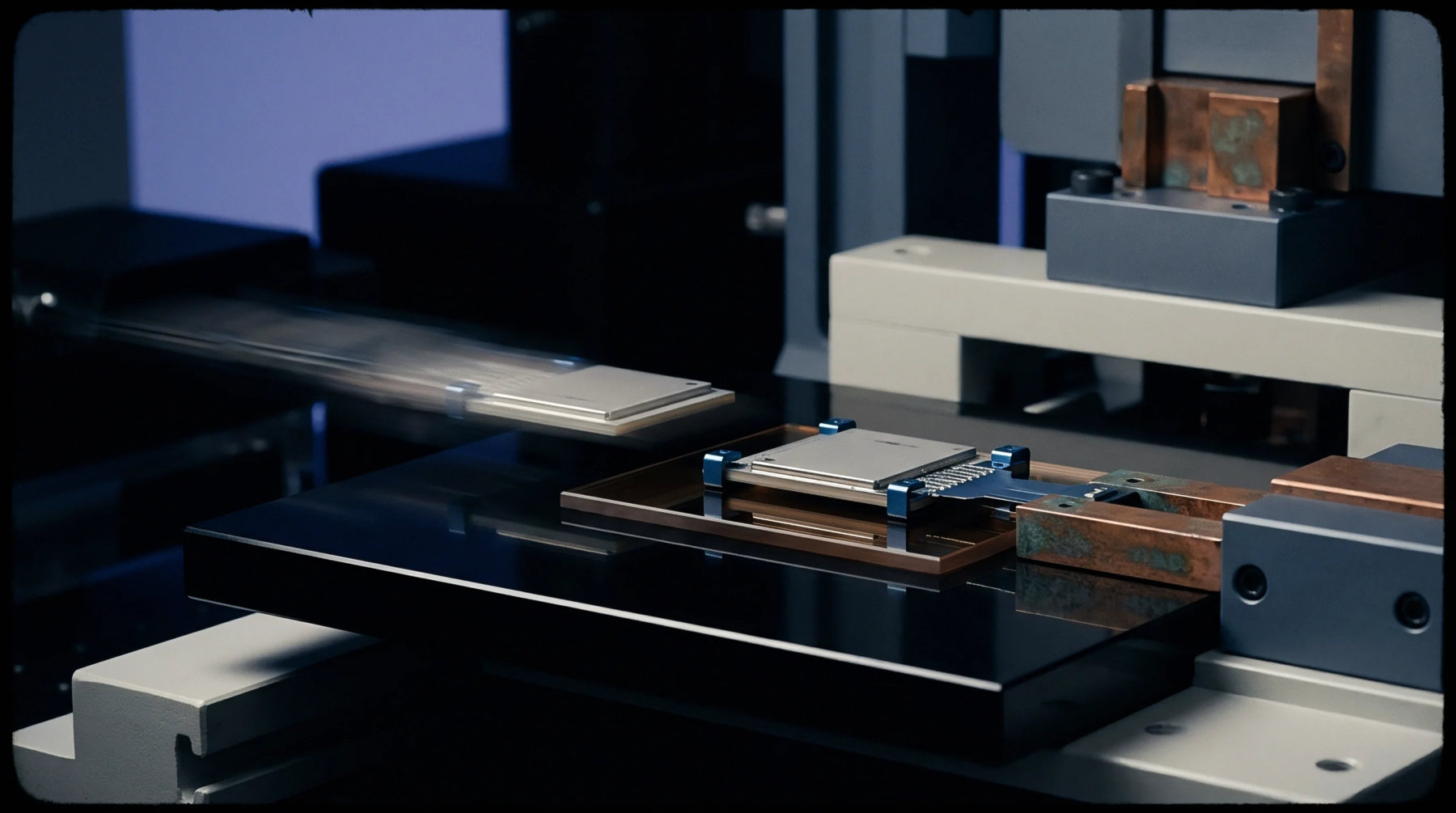
Advanced semiconductor assembly methodology positions multiple dies side by side on a high-density silicon or glass interposer to achieve high-bandwidth connectivity without full three-dimensional vertical stacking. Integrating components through this silicon interposer rather than traditional organic substrates allows 2.5d packaging to support thousands of interconnects at very tight pitches. The boundary of this technique lies at the sub-micron scaling limits where active wafer-to-wafer bonding replaces passive interposers entirely.
Substrate Integration
High-density thin-film metal layers are deposited on a supporting silicon wafer to form the routing channel. Microscopic copper pillars form the mechanical and electrical contact points between the active silicon dies and the underlying routing channels. This routing style bypasses the physical limits of standard printed circuit boards.
It allows processors and high-bandwidth memory to sit in extreme proximity.
Thermal Pathway
Heat dissipation remains a core challenge because the localized power density rises when multiple dies share a compact footprint. Dissipating power from the central processing cores requires direct thermal interface material attachment to a common metallic lid. The package is qualified by monitoring thermal resistance across the various layer interfaces during extended operation.
This qualification ensures that differences in thermal expansion do not delaminate the silicon from the interposer. When thermal stress causes different materials to expand at different rates, mechanical stress accumulates at the solder joints, requiring underfill materials to secure the connections. In high-power modules, the resulting thermal resistance must remain below a specified fraction of a degree Celsius per watt to prevent localized hot spots from degrading performance.
Defect Mitigation
Assembly yields depend heavily on the quality of known-good dies before the final integration step. Optical inspection and automated probe testing must confirm the health of each subsystem before they are placed on the interposer. When a single component is defective, the entire multi-die package is lost.
This reality pushes manufacturing standards toward zero-defect tolerances at the wafer level.