Meaning
Contact surfaces are never perfectly flat, so electrical current passes only through tiny microscopic peaks where true metal-to-metal contact occurs. Analysis of a-spot morphology reveals the physical dimensions, distribution, and geometric deformation of these micro-contacts under mechanical pressure. This surface topography determines the localized current density and contact resistance of a mating interface.
The characterization holds valid up to the melting voltage of the material, at which point thermal runaway restructures the contact zone.
Deformation Mechanism
Mechanical force applied to an electrical connection yields elastic and plastic deformation of the microscopic asperities. As the load increases, the actual contact area of a-spot morphology expands, which increases electrical pathways and decreases resistance. This mechanical transition occurs when localized stresses exceed the yield strength of the conductive material.
Degradation Pathway
Environmental exposure and thermal cycling introduce oxidation and fretting corrosion that alter the micro-contacts. When non-conductive films grow across the microscopic valleys, they restrict the active regions of a-spot morphology to even smaller zones. This restriction raises localized temperature and accelerates chemical degradation.
Contact Evaluation
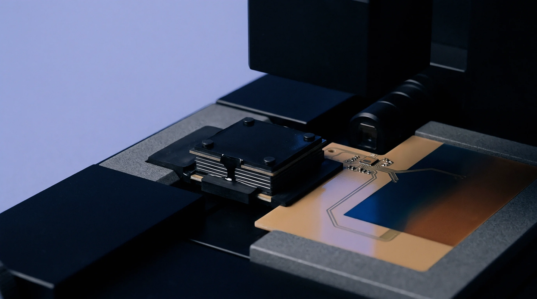
Measurement of contact resistance under varying loads provides a way to estimate the total area of the micro-junctions. High-precision digital instruments apply a controlled mechanical force to the electrical assembly while monitoring voltage drops. The extracted metrics help designers determine the clamping force required to maintain stable and low contact resistance over the lifetime of a terminal.