Meaning
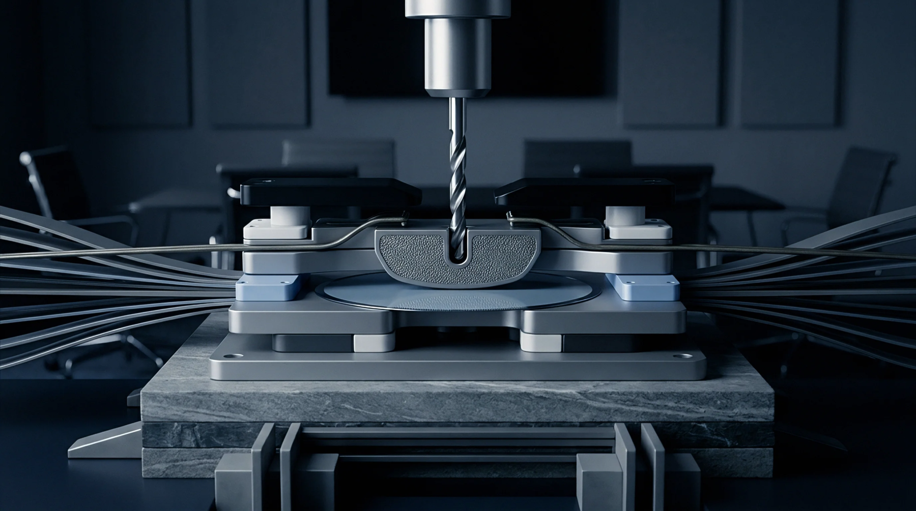
Individual functional units of semiconducting material produced by dicing a processed semiconductor wafer into discrete rectangular pieces. Within connected device manufacturing, a die contains the integrated circuits needed for processing, power management, signal routing, and wireless transmission. The boundaries of the structure are defined by scribe lines where singulation tools cut the silicon crystal.
Mechanical Specification
Physical dimensions dictate how many functional units fit onto a single silicon substrate during fabrication. Thickness variations across a bare die affect thermal transfer efficiency when mounted inside compact module packages. Edge chipping during mechanical saw singulation creates micro-cracks that compromise structural integrity under thermal shock testing.
Backside metalization layers enable low-thermal-resistance bonding to lead frames or substrate carriers. Scribe street widths are optimized to prevent active circuitry damage during high-speed laser cutting.
Assembly Integration
Pick-and-place machinery extracts validated silicon units from dicing tape using vacuum collets. Flip-chip assembly replaces wire bonds with solder bumps, reducing parasitic inductance across radio frequency interfaces. System-in-package configurations stack multiple silicon components vertically, using through-silicon vias to establish vertical interconnects between memory and logic.
Thermal expansion mismatch between the silicon body and the organic substrate requires epoxy underfill material to distribute mechanical stress. Moisture sensitivity testing confirms package integrity after surface-mount solder reflow operations.
Quality Inspection
Automated optical inspection systems scan every singulated unit for surface defects and metallization voids. Known good die testing applies temporary probe contact to confirm operating performance prior to multi-chip packaging. Electrical probing filters out defective devices before expensive encapsulation steps occur.
Failure analysis maps physical defects back to specific wafer fabrication steps to maintain process yields.