Microcontroller Die Stepping Verification during Contract Manufacturing Transfer
Verify microcontroller die steppings via automated debug register reads during transfer bring-up to prevent firmware execution failures from undocumented silicon revisions.


Silicon
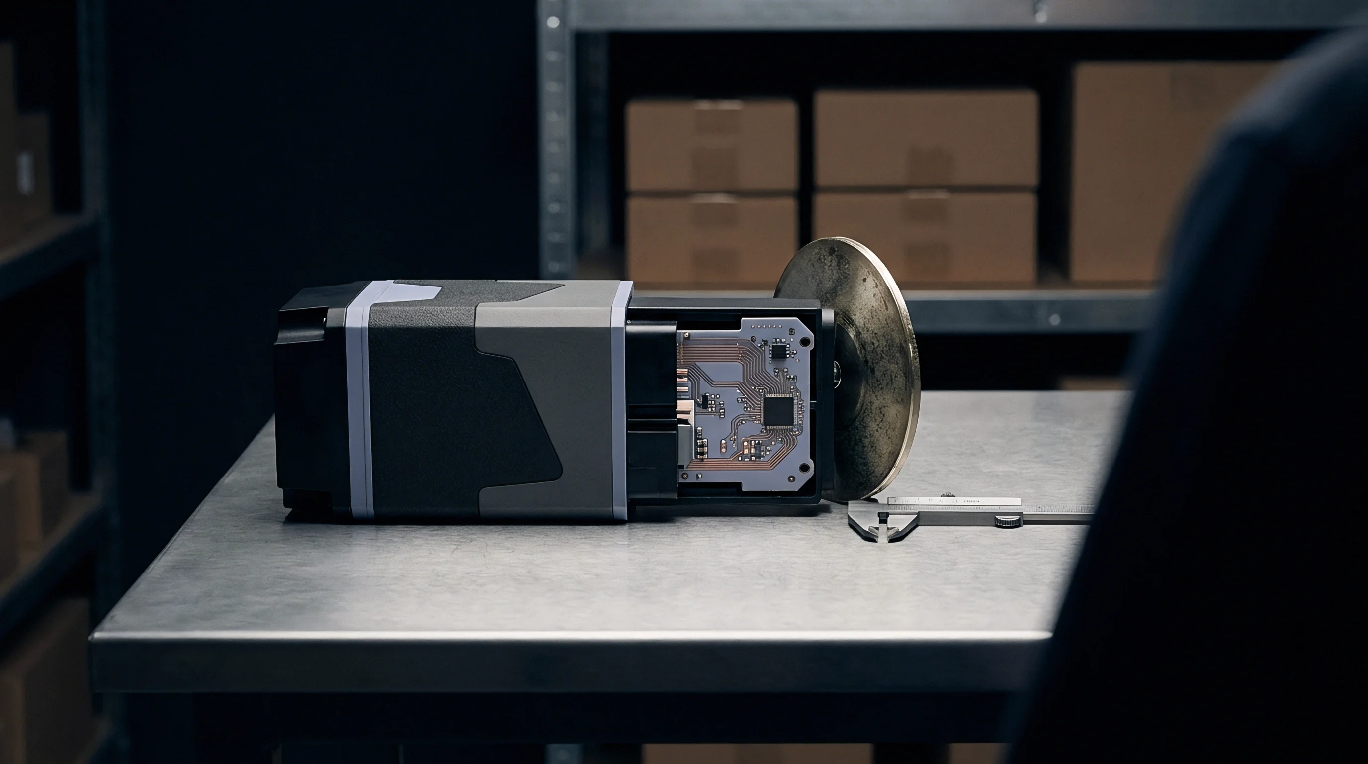
Silicon Identification Registers and Mask Revision Mechanics
Microcontroller die steppings are physical mask updates silicon foundries make to fix hardware errata, improve wafer yields, or shrink lithography. Vendors frequently release updated die revisions under identical commercial part numbers. A device labeled STMicroelectronics STM32F407VGT6 or NXP LPC55S69 can contain silicon cut A, cut B, or cut C without any change to the top-side laser marking on the quad flat package.
Inside that package, the revised silicon alters register defaults, internal flash programming algorithms, analog-to-digital converter linearity coefficients, and peripheral clock timings.
Designers hardcode revision flags directly into non-volatile register space. Microcontroller architectures provide standardized CPU identification registers alongside vendor-specific debug memory maps, allowing system developers to extract these register values via serial wire debug or during bootloader execution to identify the exact silicon stepping on the assembly line.
| Silicon Architecture | Register Address | Register Field Name | Stepping Revision Encoding | Extraction Protocol |
|---|---|---|---|---|
| ARM Cortex-M4 / M7 | 0xE000ED00 | SCB->CPUID | Bits Revision, Bits Patch | SWD / JTAG Register Read |
| STMicroelectronics STM32 | 0xE0042000 | DBGMCU_IDCODE | Bits Revision ID, Bits Device ID | SWD Read or Direct Memory Pointer |
| NXP LPC / Kinetis | 0x4001F000 | SYSCON->DEVICE_ID | Bits Silicon Revision, Bits Part ID | I2C Bootloader / JTAG Read |
| Espressif ESP32-S3 | 0x60007000 | EFUSE_BLOCK0 | Bits WAFER_VERSION_MINOR / MAJOR | eFuse Controller Read API |
| Microchip SAM D21 | 0x41008018 | DSU->DID | Bits Revision Identifier | DSU Boundary Scan / SWD Read |
The System Control Block CPUID register in ARM Cortex-M processors decodes the core design release. A value of 0x410FC241 indicates an ARM Cortex-M4 core revision r0p1, while 0x411FC241 signals revision r1p0. Vendor debug registers complement these core flags by exposing chip-level silicon modifications: the STM32 DBGMCU_IDCODE register maps directly to mask set revisions, where revision ID 0x1000 corresponds to initial Rev A silicon, 0x1001 indicates Rev Z, and 0x2000 identifies Rev Y.

Mask Set Changes and Embedded Flash Controller Variations
Die stepping changes alter internal timing constraints within the microcontroller flash memory interface. Foundry yield improvements often swap internal flash charge pumps or reduce floating-gate oxide thickness, requiring adjusted flash wait-state configurations in system clock initialization code.
ARM Cortex-M rev r1p0 silicon die revisions can alter internal flash wait-state requirements from two to three clock cycles at 120 MHz, inducing hard faults during high-temperature execution.
Firmware compiled for early silicon steppings routinely fails on updated wafer revisions when execution timing relies on unbuffered flash prefetch buffers. The microcontroller executes instructions correctly at room temperature, yet drops bus cycles when peripheral interconnect voltages droop under full load. Transferring production to a new contract manufacturer exposes these latent silicon dependencies when the plant receives a fresh wafer lot from distributors.
Minor wafer revision increments generally maintain complete pin and binary drop-in equivalence under published manufacturer datasheet specifications.
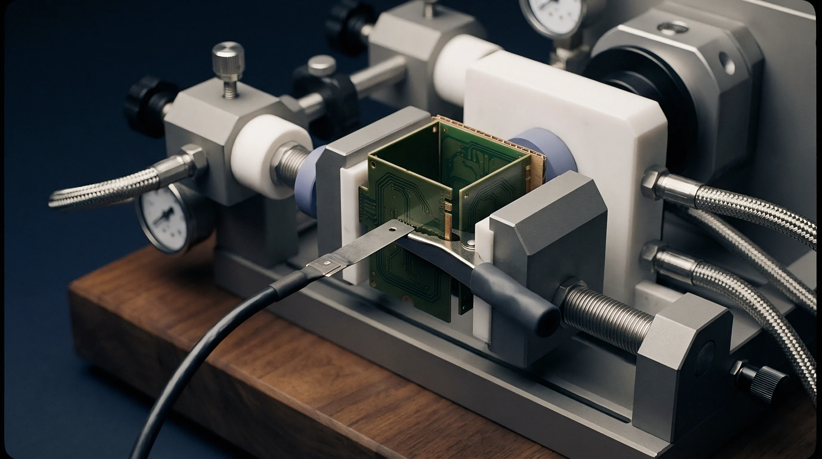

Bench

Automated Silicon Inspection Jigs on Production Lines
Contract manufacturing transfer protocols require automated die stepping audit steps integrated directly into incoming component inspection and functional board testing. Relying on contract manufacturer bill of materials audits fails because distributors fulfill reel orders using mixed date codes and varying manufacturer part suffixes.
An automated test jig validates die stepping register bytes before applying high-voltage peripheral flashing routines or executing boundary-scan passes. JTAG and Serial Wire Debug tools read CPUID, DBGMCU, and eFuse revision memory locations in under ten milliseconds during line bring-up.
- Connect target printed circuit board assembly to automated test equipment fixture via pogo-pin SWD interface.
- Apply regulated 3.3 volt target power while monitoring transient inrush current profiles.
- Halt CPU execution via SWD debug port line reset assertion within five milliseconds of power application.
- Execute JTAG or SWD memory read operation at system identification register address.
- Compare extracted CPUID and vendor revision bitfield integers against authorized design transfer package baseline files.
- Log extracted silicon stepping, serial identification code, and board serial number to factory MES database.
- Flag assembly for automated quarantine if register revision bitfields match blacklisted die steppings carrying unpatched peripheral errata.
Inline automated inspection prevents flashing invalid firmware binaries into assembled boards. Test engineers configure open-source debug tools like OpenOCD or Segger J-Link command-line scripts to dump register maps during end-of-line functional checks. Passing this register verification check releases the assembly to main bootloader application programming.

Boundary Scan and Automated Test Equipment Integration
IEEE 1149.1 boundary-scan testing isolates die stepping discrepancies at the physical silicon interface. Component boundary-scan description language files define test access port registers and device identification codes. When a silicon foundry alters internal pad layout geometries or updates bond wire interconnect paths during a die shrink, the TAP controller IDCODE register changes its hardware bitmask.
ISO 12207 configuration management provisions establish that altering an MCU die stepping without re-validating timing boundaries invalidates the transferred assembly functional safety certification.
Functional test engineers integrate silicon revision extraction routines into automated test equipment jigs using structured JSON or XML script outputs. The test bench logs silicon revision strings alongside board barcode identifiers to maintain complete traceability across manufacturing transfer batches. When a functional test failure occurs, component trace logs isolate whether failure rates cluster around specific silicon stepping dates.
Standard IPC-1791 Section 5.2 clauses specify that any silicon die revision change demands written baseline re-authorization before production lot release.


Divergence

Hardware Errata Variations across Wafer Revisions
Microcontroller errata sheets document peripheral silicon flaws discovered during mass production. Semiconductor manufacturers issue stepping updates specifically to resolve critical errata, yet these fixes frequently alter peripheral timing behaviors or remove software workarounds implemented in legacy firmware stacks.

Which Silicon Register Fields Reveal Stepping Revision Shifts?
Register fields in core system control blocks, vendor debug modules, and feature configuration fuses expose die revision shifts. Reading ARM Cortex-M SCB CPUID bits 3 through 0 reveals patch levels, while vendor-specific registers like ST DBGMCU_IDCODE or NXP SYSCON DEVICE_ID capture chip-level mask updates. Flash memory controller ID registers and factory eFuse registers similarly reflect underlying lithography changes.
| Peripheral Module | Die Stepping Shift | Hardware Failure Mode | Firmware Remediation Requirement |
|---|---|---|---|
| Flash Memory Controller | Rev A to Rev B (Die Shrink) | High-temperature write corruption during internal charge pump operation. | Update flash program wait-state bitfields in system clock initialization routine. |
| Direct Memory Access (DMA) | r0p1 to r1p0 Core Update | Bus matrix arbitration deadlock during simultaneous UART and SPI transfers. | Implement burst-length caps in DMA channel control registers. |
| Analog-to-Digital Converter | Cut 1 to Cut 2 Mask Fix | Internal bandgap reference voltage drift exceeding datasheet limits by 4%. | Reload factory calibration vectors from system memory sector into firmware scaling math. |
| Universal Asynchronous Receiver | Rev 1 to Rev 3 Silicon | Auto-baud rate detection lockup upon receiving framing error bytes. | Clear software error flags manually via interrupt service routine conditional check. |
| Low-Power Sleep Modes | Step 0 to Step 1 Wafer | Deep-sleep wake-up timer interrupt fails to re-enable high-speed crystal oscillator. | Reconfigure power management unit delay registers prior to sleep entry. |
Firmware written for early silicon steppings often contains custom register patches designed to bypass silicon bugs. When a contract manufacturer builds boards using updated die steppings where the silicon bug is permanently resolved, legacy software workarounds cause unexpected system lockups or memory access violations.
Treat every silicon stepping change as an unvetted microcontroller swap until register verification and boundary-scan tests prove peripheral errata equivalence.
- DMA Arbitration Deadlocks occur when updated bus matrix priorities cause memory starvation on high-speed peripheral channels.
- Internal Oscillator Drift manifests when modified trimming resistor ladders shift system clock frequencies beyond USB bus timing tolerances.
- GPIO Drive Strength Anomalies emerge when die shrink lithography alters gate oxide capacitance, causing signal ringing on fast SPI busses.
- Spurious Reset Assertion happens when updated brown-out detector circuits respond to power supply noise pulses previously filtered by parasitic chip capacitance.
Silicon revisions introduce peripheral timing shifts that evade short-term functional testing. Embedded systems can fail after weeks in field deployment due to subtle race conditions created by altered internal bus arbitration logic.
Bypassing die stepping qualification during manufacturing transfer compromises product reliability and triggers immediate field return penalties under contractual warranty obligations.


Escrow

Configuration Control and Transfer Documentation Packages
Contract manufacturing transfer packages require complete silicon configuration custody files. Sourcing teams build hardware data packages containing explicitly documented silicon revision dependencies alongside Gerber layout files, bill of materials documents, and firmware source repositories. Establishing precise stepping records prevents contract manufacturers from substituting alternative silicon stocks to bridge component supply gaps.
Contract manufacturers routinely source older die steppings from grey-market distributors to cover line shortages during transfer bring-up without logging an engineering change request.
Software build systems must incorporate conditional macro definitions that parse silicon CPUID register values at runtime or compile binaries specific to target silicon revisions. Hardware abstraction layers (HAL) supplied by chip vendors frequently drop support for legacy die steppings in newer driver software development kit releases. Sourcing practices must archive the exact software toolchain versions used during original product qualification.
- Silicon Revision Matrix File maps approved silicon mask revisions against authorized firmware version releases and peripheral configuration flags.
- Part Change Notification Registry tracks all vendor PCN notices issued against the microcontroller part family across the product lifecycle.
- Vendor Software SDK Escrow stores compiled static libraries, board support packages, and linker scripts configured for target die steppings.
- Factory Flashing Script Package specifies OpenOCD, J-Link, or Cyclone programmer scripts equipped with silicon register validation macros.
Establishing clear escrow parameters protects intellectual property and hardware build integrity. The transfer package defines explicit boundary specifications for acceptable silicon steppings on all target board assemblies.
Silicon vendor lifecycle guarantees bind component availability rather than stepping persistence on the assembly bill of materials.
Penalty

Commercial Liability and Non-Recurring Engineering Allocation
Unannounced die stepping swaps during manufacturing transfers generate substantial financial costs. When a contract manufacturer builds thousands of board assemblies using unvetted silicon steppings, the buyer faces board scrap costs, line downtime, and engineering re-qualification charges. Contract agreements must explicitly allocate these commercial risks between the sourcing buyer and the manufacturing service provider.
| Transfer Phase / Event | Responsible Party | NRE Cost Metric | Commercial Consequence |
|---|---|---|---|
| Unannounced Silicon Substitution | Contract Manufacturer | Full Lot Scrap + Material Overhead | CM absorbs 100% replacement assembly and component acquisition costs. |
| Silicon Errata Qualification | Sourcing Buyer | $8,000 to $25,000 Engineering Fees | Buyer pays for test bench scripting and firmware patch validation. |
| Factory Line Stoppage Delay | Contract Manufacturer | $1,500 per Line Hour Downtime | CM forfeits scheduling delay claims if unvetted silicon caused stoppage. |
| Functional Safety Re-Certification | Shared Allocation | $40,000 to $120,000 Lab Fees | Cost split based on PCN notification compliance history. |
Manufacturing contracts must mandate that contract facilities submit formal engineering change requests (ECR) prior to loading alternative microcontroller lot date codes onto surface mount production lines. Sourcing terms dictate that assemblies loaded with unauthorized die steppings are subject to immediate commercial lot rejection.
Non-recurring engineering costs accrued during silicon re-qualification become non-recoverable when manufacturing transfer agreements lack explicit component change notification liabilities.
Clear financial boundaries enforce compliance across offshore manufacturing facilities. Sourcing managers enforce component auditing protocols to verify every semiconductor lot delivered to the assembly plant floor.
Whether contract manufacturing agreements can legally bind secondary wafer foundries to preserve legacy mask steppings when primary fab lines transition to smaller geometry nodes remains unsettled across cross-border assembly jurisdictions.