Meaning
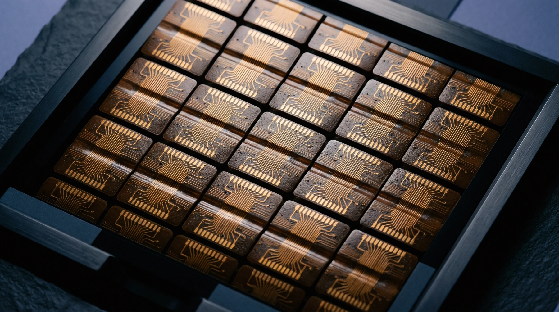
Additional thin-film metal and dielectric layers on a silicon die rearrange the contact pads to match the bump pattern of a flip chip assembly. This layout, known as flip chip RDL, routes the signals from the peripheral pads of the die to an area array of solder bumps. This design allows for higher interconnect density and better electrical performance.
Metal Layer
Thin copper traces are sputtered and electroplated on the passivation layer of the silicon wafer to establish the new circuits. This fabrication of flip chip RDL allows the design team to optimize the power distribution network by widening the ground and supply lines. This layer acts as a buffer against mechanical strain during thermal cycling, which reduces the risk of delamination at the die interface under extreme conditions.
Thermal Path
Direct attachment of the die to the substrate removes the need for long bond wires that introduce unwanted inductance. This electrical path created by flip chip RDL minimizes signal degradation in high-frequency applications. Signal integrity is therefore preserved.
Packaging Efficiency
Modern mobile processors rely on these structures to squeeze more functionality into extremely thin form factors. This adoption of flip chip RDL enables multi-die integration within a single package, which reduces the overall footprint of the system on the motherboard. This integration represents the standard path for next-generation hardware designs.