Meaning
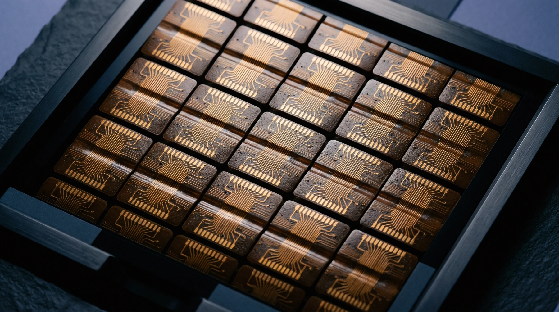
Slow atomic displacement of copper metallization in microelectronic interconnects under electrical and thermal stress defines the electrochemical migration of bonding elements. This phenomenon, known as copper wire drift, occurs when electrical current densities and operating temperatures exceed safe operating limits, leading to void formation or short circuits. Device behavior becomes unstable over long periods of operation.
Reliability Risk
Elevated temperatures accelerate the diffusion of copper atoms into adjacent semiconductor layers. The absence of effective barrier layers allows copper wire drift to alter the electrical characteristics of the junction, eventually leading to catastrophic dielectric breakdown. Packaging materials must be selected to withstand this thermal stress.
Degradation Phase
Microstructural changes occur in stages as the metallic ions migrate along grain boundaries. Initial phases of copper wire drift produce subtle shifts in contact resistance that may bypass early quality control screens. Later stages exhibit localized fractures or resistive paths.
Measurement Protocol
Accelerated life testing evaluates the rate of copper wire drift through continuous high-temperature bias stress. Practitioners measure leakage current across test structures at regular intervals to establish the onset of wearout. This quantitative evaluation determines the overall lifespan of the integrated circuit, which helps designers adjust the current density budgets for the silicon layout before the tape-out process begins.