Meaning
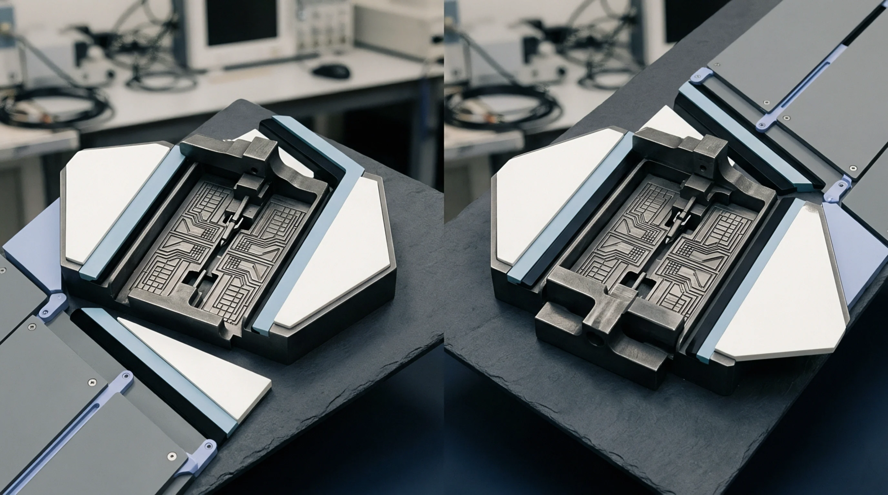
Specialized board validation methodologies evaluate the electrical integrity of printed circuit assemblies with extremely narrow trace widths and closely spaced contact pads. Applying high density circuit testing ensures that complex multilayer boards used in compact communication devices are free from micro-shorts and open circuits. It relies on advanced physical probes or optical inspection systems.
Probing Precision
Using physical contacts on miniature test pads requires high mechanical precision. Conventional spring loaded pins are often too large for boards with sub-millimeter spacing, which necessitates the use of fine pitch probe cards or flying probe testers. These specialized systems make contact without scratching or bending the delicate circuit traces.
Diagnostic Technology
Alternative approaches to electrical validation rely on non-contact or automated optical methods to find defects. Automated optical inspection scans the board surface for solder bridges, while boundary scan testing uses integrated logic inside the active components to verify trace routing electronically. In high volume manufacturing, a combination of flying probe and boundary scan delivers thorough coverage.
This dual strategy identifies microscopic solder voids and insulation breakdowns before the board is mounted in its metal enclosure.
Production Integration
Incorporating complex diagnostic steps into the assembly line demands careful balance between inspection depth and cycle time. High speed boundary scan routines can run in seconds, whereas physical flying probes take minutes per board. Engineers select the specific combination that minimizes total cycle time while maintaining high quality standards.