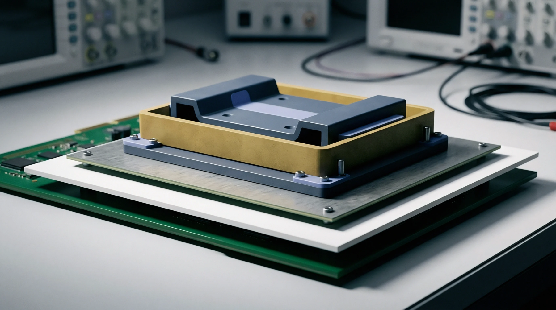
Mould and Test Jig Ownership When Production Moves
Asset ownership requires unbundled NRE contracts, native CAD databases, containerized firmware build tools, and explicit bailment agreements waiving factory liens.
Solder paste inspection standard defines the requirements for measuring the volume, area, and height of solder deposits on a printed circuit board to identify defects before component placement. This measurement is performed by an automated optical system that uses structured light or laser sensors to create a three dimensional map of the solder on the pads. By following the spi class 101 guidelines, the manufacturing team can ensure that the correct amount of paste is applied to every pad, which is critical for preventing solder bridges or insufficient joints.
This step in the process is highly effective because it catches errors at the earliest possible stage, where they are much cheaper to fix. If the inspection fails, the board can be wiped clean and reprinted in a matter of minutes. This standard is a key part of any high quality surface mount technology production line.
Measurement of the exact quantity of solder paste is the most important task of the inspection system. Under the spi class 101 framework, the volume of the paste is compared to the theoretical volume of the stencil aperture. If the volume is too low, the resulting joint may be weak or open, leading to an electrical failure.
Conversely, too much paste can cause short circuits between adjacent pads, especially on fine pitch components. The system calculates the volume by integrating the height measurements across the entire area of the pad. This three dimensional analysis is much more reliable than older two dimensional methods that only measured the area of the paste.
Maintaining a high level of volumetric accuracy is the first step in achieving a high first pass yield.
Identification of common printing errors allows the production team to adjust the screen printer before a large batch of boards is affected. The spi class 101 standard includes specific criteria for identifying defects such as bridging, smearing and misalignment. If the paste is shifted too far to one side, the component will not sit correctly on the pads, leading to a defect called tombstoning.
The software can also detect when the stencil is becoming clogged, as the volume of the deposits will gradually decrease over several boards. By catching these problems in real time, the factory can maintain a high level of quality without stopping the line for long periods. This proactive approach to quality control is essential for high volume manufacturing.
Statistical analysis of the inspection data provides a way to monitor the stability of the entire printing process over time. In the context of spi class 101, the system tracks the trends in the volume and height measurements to identify when the process is starting to drift. For example, if the average height of the solder paste begins to increase, it might indicate that the stencil is wearing out or that the paste is drying out.
These early warning signs allow the technicians to perform maintenance before any actual defects occur. The data can also be used to compare the performance of different solder pastes or stencil technologies. This continuous improvement loop ensures that the production line remains efficient and reliable.
Successful implementation of this standard provides the data needed to optimize the printing process for every new board design.
Asset ownership requires unbundled NRE contracts, native CAD databases, containerized firmware build tools, and explicit bailment agreements waiving factory liens.
Expertise is a utility, not a secret. sentiention™ publishes its working knowledge as open reference: intelligence layer covering the materials it sources, the markets it enters, and the reference that serves both.