Meaning
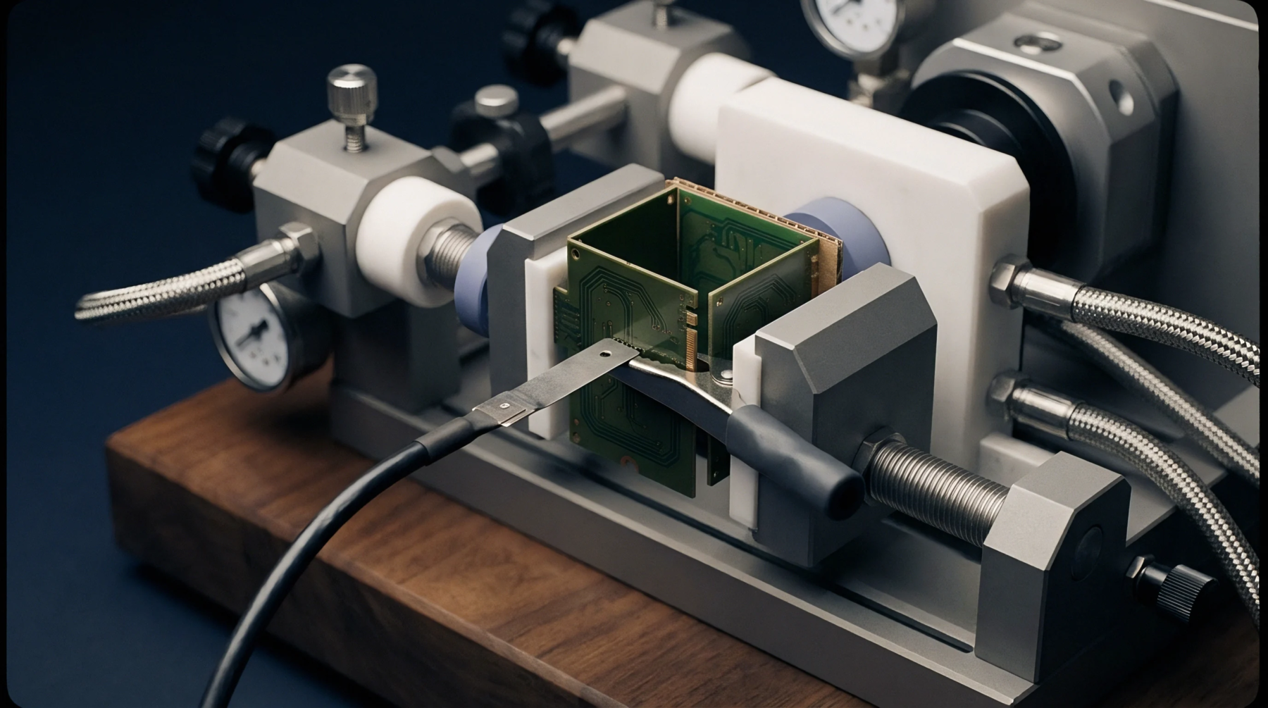
Electrical testing identifies functional integrated circuits on a semiconductor wafer before the silicon is sliced into individual chips. A wafer probe sort involves moving a set of fine needles across the surface to contact the bond pads of each die. This stage prevents the expense of packaging defective components that failed during the manufacturing process.
Contact Quality
Maintaining a low-resistance connection between the probe tips and the aluminum or copper pads is necessary for accurate measurement. The wafer probe sort requires precise mechanical alignment to avoid damaging the delicate structures on the die. Debris on the probe card or uneven force can lead to false failures or intermittent readings.
Binning Strategy
Tested dies are categorized based on their performance characteristics such as maximum clock frequency or power consumption. The wafer probe sort generates a map that guides the assembly house in selecting parts for different product grades.
Retest Protocol
Marginal failures are often checked a second time to confirm the result was not caused by a poor mechanical connection or transient noise. Refining the results in this manner helps maximize the recovery of functional silicon that would otherwise be discarded as scrap. Advanced systems use temperature-controlled chucks to verify that the circuits operate correctly at both the hot and cold extremes of the specification before the wafer proceeds to the dicing stage.