Silicon Wafer Processing and Substrate Dielectric Degradation Mechanisms
Substrate dielectric degradation reduces RF transceiver link budgets over time, requiring a minimum four-decibel margin allowance during module procurement.

Substrate
Bench testing an RF transceiver at 915 MHz often turns up performance gaps that standard datasheets don’t capture. High-resistivity silicon wafers ~ specified above 1000 ohm-centimeters bulk resistivity ~ suffer from surface conduction when ambient dielectric charges accumulate. Right under the thermally grown silicon dioxide passivation layer, fixed oxide charges induce an inversion or accumulation channel in the silicon.
This thin conductive layer acts as a parasitic resistance. RF signals moving through integrated passive devices, microstrip lines, or switch FETs couple right into this inversion layer. That energy loss degrades receiver sensitivity and burns off transmit power as heat before it ever reaches the antenna port.
Substrate loss is one of the main reasons link budgets erode over time in high-frequency wireless systems. For radio modules destined for long deployments, RF performance hangs on the structural integrity of that dielectric-silicon interface. Standard bulk CMOS leaves unsaturated dangling bonds at the interface ~ what datasheets track as interface trap density.
Under constant electric field bias, these trap states exchange charge with the semiconductor bulk, shifting the local dielectric constant and altering parasitic capacitance under signal traces.

High Resistivity Silicon Wafers for Radio Frequency Devices
RF-SOI technology mitigates substrate loss by inserting a buried oxide dielectric layer between the thin active silicon and the bulk silicon substrate. Beneath that buried oxide, high-resistivity substrates typically run between 1000 and 5000 ohm-centimeters. But standard silicon processing introduces thermal donors during ingot pulling and wafer annealing; without tight control over thermal budgets, bulk resistivity can collapse down to 50 ohm-centimeters.
Batch evaluations of RF-SOI switches trace attenuation spikes directly to thermal donor formation in the wafer. As bulk resistivity drops, substrate dielectric losses scale up with signal frequency. At 2.4 GHz, a drop from 2000 ohm-centimeters down to 100 ohm-centimeters adds 0.45 dB of insertion loss across an integrated transmit switch.
Across a multi-stage power amplifier output network, that extra loss eats into battery life and drives up operating temperatures.
RF Trap Layers and Surface Conduction Channels
Stopping surface conduction under the oxide requires additional processing steps at the foundry. Fabricators deposit a trap-rich layer of polysilicon ~ packed with high-density grain boundaries ~ between the high-resistivity substrate and the buried oxide layer. This trap-rich layer pins the Fermi level and neutralizes fields created by fixed oxide charges.
Free carriers generated by oxide charges get caught in the polysilicon grain boundaries, maintaining high substrate resistivity right at the dielectric boundary.
Without a reliable trap-rich layer, large RF voltage swings trigger non-linear surface conduction. High-power transmit bursts generate second- and third-harmonic distortion directly within the substrate. In sub-GHz radios pushing 27 dBm output, unpassivated substrate dielectrics create second-harmonic spurs at -55 dBc.
Adding a passivated trap-rich substrate suppresses those harmonics below -85 dBc, keeping intermodulation out of adjacent receiver bands.
Substrate Parasitic Capacitance and Signal Attenuation
Dielectric wear changes the parasitic capacitance between RF interconnects and the ground plane beneath them. Oxide capacitance per unit area comes down to dielectric thickness and relative permittivity ~ thermal silicon dioxide holds at 3.9. However, processing swings, hydrogen exposure, or defect trapping shift these local dielectric properties, introducing phase variations along high-frequency signal traces.
Substrate interface degradation manifests in several distinct failure modes across wireless hardware.
- Harmonic Distortion Spikes occur when charge building up beneath gate dielectrics shifts substrate capacitance during high-power RF voltage swings.
- Receiver Noise Figure Elevation occurs when localized thermal noise from low-resistivity conduction paths couples directly into LNA inputs.
- Phase Locked Loop Instability happens when charge trapped in the dielectric alters parasitic capacitance inside VCO tuning circuits.
- Transceiver Sleep Leakage Expansion stems from dielectric breakdown along isolation wells, opening sub-threshold leakage paths across power domains.
Evaluating high-resistivity wafers means measuring small-signal insertion loss and large-signal harmonic distortion across temperature sweeps. Standard acceptance testing often relies on low-frequency capacitance-voltage curves, which miss high-frequency surface conduction channels entirely. RF teams need to mandate high-frequency microstrip resonator tests on incoming silicon lots to confirm dielectric stability.
Whether trap-rich polysilicon layers can retain their defect density over decades of thermal cycling without dumping trapped charges back into the conduction channel remains an unsettled question for long-life hardware procurement.


Oxidation
Growing high-quality oxide films on silicon is fundamental to semiconductor fabrication. In thermal oxidation, wafers react with dry oxygen or water vapor inside high-temperature furnaces kept between 800 and 1100 degrees Celsius. Dry oxidation forms dense silicon dioxide films with high breakdown voltages ~ ideal for thin gate insulators.
Wet oxidation grows much faster, yielding the thicker field oxides used for device isolation and inter-metal dielectrics.
As thermal oxidation proceeds, silicon atoms consume incoming oxygen at the moving boundary, expanding the volume by roughly 2.25 times compared to the original silicon. This physical expansion builds up heavy compressive stress within the growing oxide film. Residual mechanical stress at the interface distorts the energy band structure, introducing localized energy states into the silicon bandgap.
Thermal Oxide Growth Kinetics and Interface Trap Formation
Thermal oxide growth kinetics follow the Deal-Grove model, balancing surface reaction rates against diffusion rates through the growing film. For thin gate oxides under 10 nanometers, initial growth follows linear kinetics governed by surface reaction rates. Interface state density (Dit) tracks directly with growth temperature, ambient atmosphere during oxidation, and downstream annealing routines.
Unpassivated silicon bonds at the interface ~ trivalent silicon defects, or Pb centers ~ act as active charge traps. Post-oxidation annealing in hydrogen or forming gas at 400 to 450 degrees Celsius passivates these dangling bonds by creating silicon-hydrogen (Si-H) bonds. But Si-H bonds have lower dissociation energy than Si-Si or Si-O bonds.
Under electrical or thermal stress, these bonds split, releasing hydrogen and reforming interface traps that degrade transconductance.
Passivating interface traps with deuterium instead of hydrogen increases bond dissociation energy and extends dielectric operating life under RF stress.
High-K Dielectric Stacks in Sub-22nm RF CMOS
Sub-22nm RF transceivers replace pure silicon dioxide gate dielectrics with high-permittivity (high-k) materials like hafnium dioxide (HfO2) or hafnium silicate (HfSiO). These materials allow greater physical thickness for a given equivalent oxide thickness (EOT), curbing direct quantum tunneling leakage. That added physical thickness keeps gate leakage from bleeding off micro-ampere battery budgets in low-power wireless nodes.
Depositing hafnium dioxide onto silicon requires an ultrathin silicon dioxide or silicon oxynitride interfacial layer to preserve carrier mobility in the channel. This dual-layer stack creates complex degradation pathways: charge traps accumulate at the boundary between the silicon dioxide and hafnium dioxide layers, while oxygen vacancies in the hafnium oxide act as bulk electron traps, shifting threshold voltage under sustained DC bias and RF excitation.
Plasma-Enhanced CVD Dielectrics for Interlevel Metallization
Back-end-of-line (BEOL) processing relies on plasma-enhanced chemical vapor deposition (PECVD) for interlevel dielectric layers between metal interconnects. PECVD films ~ such as silicon oxynitride (SiON) and carbon-doped silicon dioxide (SiCOH) ~ are deposited between 300 and 400 degrees Celsius to keep aluminum or copper metallization from melting.
Because of these lower temperatures, PECVD films are less dense and carry more hydrogen than thermal oxides. They retain higher levels of precursor residues, silanol groups (Si-OH), and structural nanopores. When high-frequency RF signals travel through copper traces, electric fields penetrate the adjacent low-k dielectric; any absorbed moisture or silanol dissociation elevates the loss tangent, attenuating signals through multi-layer interconnect networks.
| Node Technology | Dielectric Material | Physical Thickness | Dielectric Constant | Breakdown Field | Primary Trap Mechanism |
|---|---|---|---|---|---|
| 180 nm Planar CMOS | Thermal SiO2 | 3.5 nm | 3.9 | 11.0 MV/cm | Interfacial Si-H Dissociation |
| 65 nm RF CMOS | Silicon Oxynitride | 1.8 nm | 4.2 | 10.2 MV/cm | Nitrogen-Related Electron Traps |
| 22 nm Planar FD-SOI | HfO2 / SiO2 Stack | 1.2 nm (EOT) | 18.0 (HfO2) | 8.5 MV/cm | Bulk Oxygen Vacancy Trapping |
| 16 nm FinFET RF | HfZrOx / SiON Stack | 0.95 nm (EOT) | 22.0 (HfZrOx) | 7.8 MV/cm | Pre-existing Outer Interface Traps |
| Data measured at 25 degrees Celsius; breakdown field defined at 1 mA/cm2 leakage threshold under DC ramp. | |||||
Controlling furnace thermal budgets during oxide growth helps limit stress buildup and trap density across the wafer.
While high thermal budgets clear out physical defects, they risk redistributing dopants within active device channels.

Stress
Electrical bias and heat drive dielectric degradation over time. Applying an electric field across a thin gate oxide sets up steep potential gradients, accelerating electrons and holes through the conduction band or pushing them into localized defect states. Over years of field operation, this continuous bombardment breaks atomic bonds, generating new traps and permanently shifting operating parameters.
In wireless SoC devices, dielectric wear shows up as parameter drift: power amplifiers, VCOs, and low-noise amplifiers suffer bias shifts, reduced gain, and higher phase noise. Evaluating this under real-world conditions requires isolating individual stress mechanisms and assessing how their combined effects hit system performance.
Bias Temperature Instability in Deep Submicron RF Transceivers
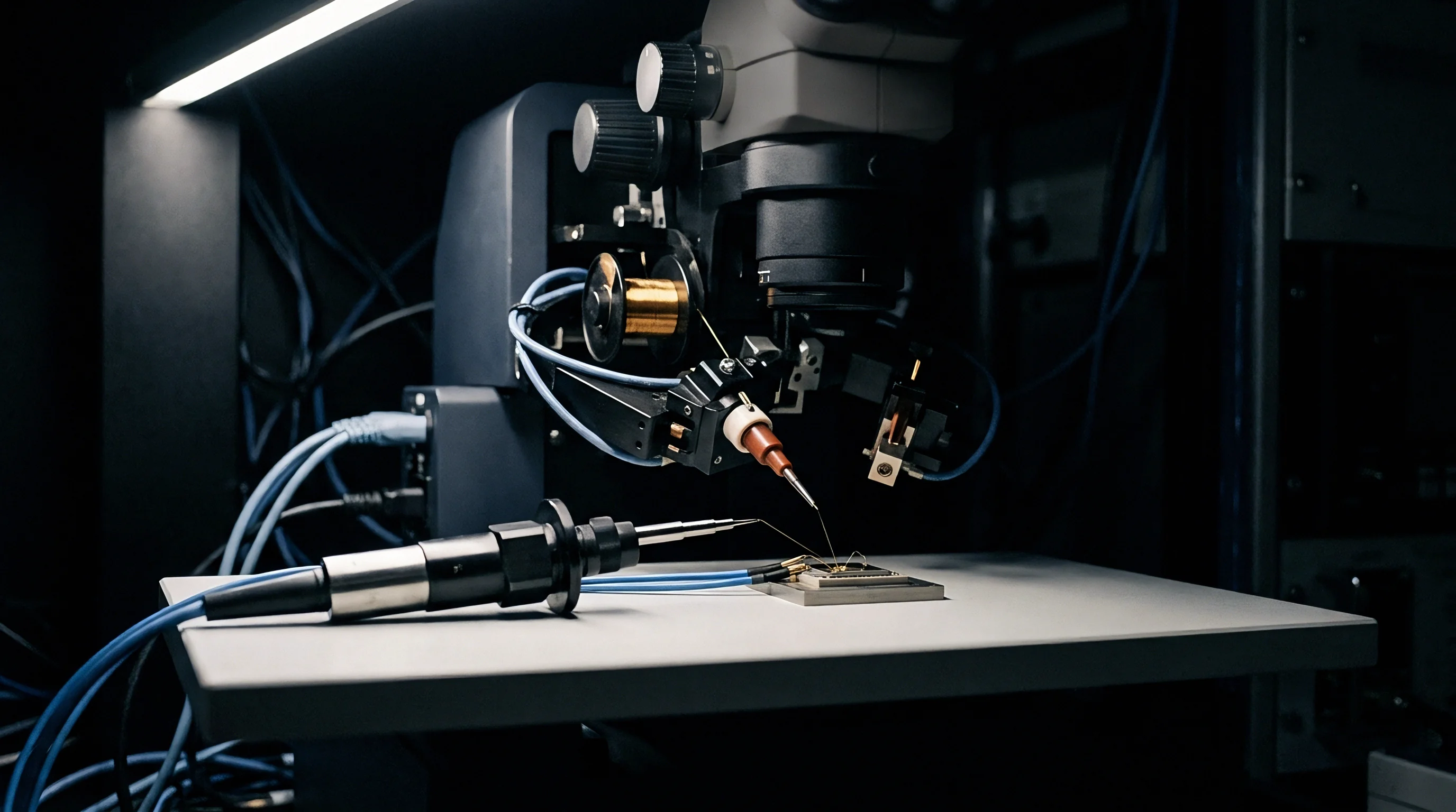
Negative Bias Temperature Instability (NBTI) affects p-channel MOSFETs operating under negative gate-to-source bias at elevated temperatures. The electric field pulls holes toward the gate interface, where energetic carriers break silicon-hydrogen bonds. This creates donor-type interface traps and releases neutral hydrogen, which diffuses into the bulk oxide.
Positive Bias Temperature Instability (PBTI) affects n-channel MOSFETs with high-k metal gate stacks. Under positive gate bias, electrons tunnel from the inverted channel into pre-existing oxygen vacancies within the hafnium oxide. PBTI causes a positive threshold voltage shift (Δ Vth), cutting drain current and transconductance (gm).
In an LNA, that loss of gm degrades overall RF gain and raises input-referred noise.
The threshold voltage shift over time follows a standard power-law relationship:
Δ Vth(t) = A · exp(γ · Eox) · expleft(-fracEakB Tright) · tn
Here A is a process-dependent pre-factor, Eox represents the gate oxide electric field, γ is the field acceleration parameter, Ea is the activation energy (typically 0.1 to 0.2 eV for NBTI relaxation components), kB is Boltzmann’s constant, T is temperature in Kelvin, and n is the time exponent (typically 0.16 to 0.25).
Continuous DC gate stress of 1.8 MV/cm at 125 degrees Celsius for 1000 hours induces a 38 mV threshold voltage shift in unpassivated pMOS switches.
Hot Carrier Injection Mechanics in Microwave Power Amplifiers
Hot Carrier Injection (HCI) occurs when high drain-to-source voltages accelerate carriers toward the drain pinch-off region. Electrons or holes gain enough energy to clear the silicon-dioxide potential barrier (3.2 eV for electrons, 4.7 eV for holes) and inject directly into the gate dielectric.
HCI wear accelerates in RF power amplifiers operating in saturation, where high voltage swings across the drain subject carriers to peak electric fields twice per carrier cycle. Hot carriers create interface traps and fixed charges near the drain edge of the gate, leading to asymmetric transconductance loss that shifts optimum load matching and degrades saturated output power (Psat) over time.
Wafer Level Reliability Test Protocols for RF Dielectrics
Confirming dielectric integrity requires standardized wafer-level stress testing before dies are packaged into modules.
- Position incoming unpassivated test wafers on an automated temperature-controlled probe station set to 125 degrees Celsius.
- Probe dedicated test structures ~ including gate-controlled diodes, large-area oxide capacitors, and RF switch transistors ~ using ground-signal-ground probe tips.
- Record baseline parameters: initial gate leakage, drain current, threshold voltage, and small-signal scattering parameters (S11, S21) up to 10 GHz.
- Apply constant voltage bias stress across gate oxides at 1.3 times nominal operating electric field, keeping source, drain, and bulk terminals grounded.
- Pause stress application at logarithmic intervals (1s, 10s, 100s, 1000s) to log parameter shifts while keeping recovery time to a minimum.
- Extract activation energies and field acceleration parameters by repeating the stress sequence at 85, 125, and 150 degrees Celsius.
Premature NBTI shifts in unscreened wafer lots have forced recalls of 12,000 sub-GHz gateway units installed in remote utility cabinets, costing over forty thousand dollars.


Breakdown
Dielectric breakdown is the ultimate destruction of an oxide’s insulating properties under stress. Microscopic defects accumulate in the bulk oxide over time, driven by electric field strength, operating temperature, and current flow. When defect density reaches a critical threshold, a conductive path bridges the dielectric, turning the insulating film into a resistive short.
In integrated circuits, breakdown occurs in two distinct phases: soft breakdown and hard breakdown. Soft breakdown happens when a localized filament of high defect density forms; leakage current jumps in steps, but the circuit remains partially functional. Hard breakdown follows when thermal runaway along that filament melts surrounding dielectric and metallization, triggering total failure.

Time-Dependent Dielectric Breakdown in Thin Gate Insulators
Time-Dependent Dielectric Breakdown (TDDB) sets the operational lifespan of gate oxides and MIM capacitors in RF front-end chips. Percolation theory explains how defects spread through the oxide matrix: as traps accumulate randomly, neighboring defects begin to overlap. When a continuous chain of overlapping traps reaches from the gate electrode to the substrate channel, percolation completes.
The time to breakdown (tbd) follows a Weibull distribution:
F(t) = 1 – expleft( -left( fractη right)β right)
Here η represents the characteristic time to breakdown at 63.2 percent cumulative failure, and β is the Weibull shape parameter. Thinner oxides exhibit lower β values, which spreads the statistical failure distribution and increases early-life failure probability in large-area ICs.

How Does Charge Trapping Shift Oscillator Phase Noise?
Defect traps inside gate oxides act as generation-recombination centers that produce low-frequency 1/f flicker noise. In a voltage-controlled oscillator (VCO), transistor non-linearities up-convert this flicker noise to offset frequencies right around the RF carrier. Charge trapping in the dielectric directly degrades phase noise.
As TDDB advances toward soft breakdown, trap generation drives up gate leakage noise spectral density. This low-frequency noise modulates both varactor capacitance and transistor transconductance in the VCO tank. Transceivers undergoing soft breakdown show elevated close-in phase noise, which degrades receiver adjacent-channel selectivity and raises bit error rates in high-order modulation schemes.
Soft Breakdown Progression to Hard Catastrophic Failures
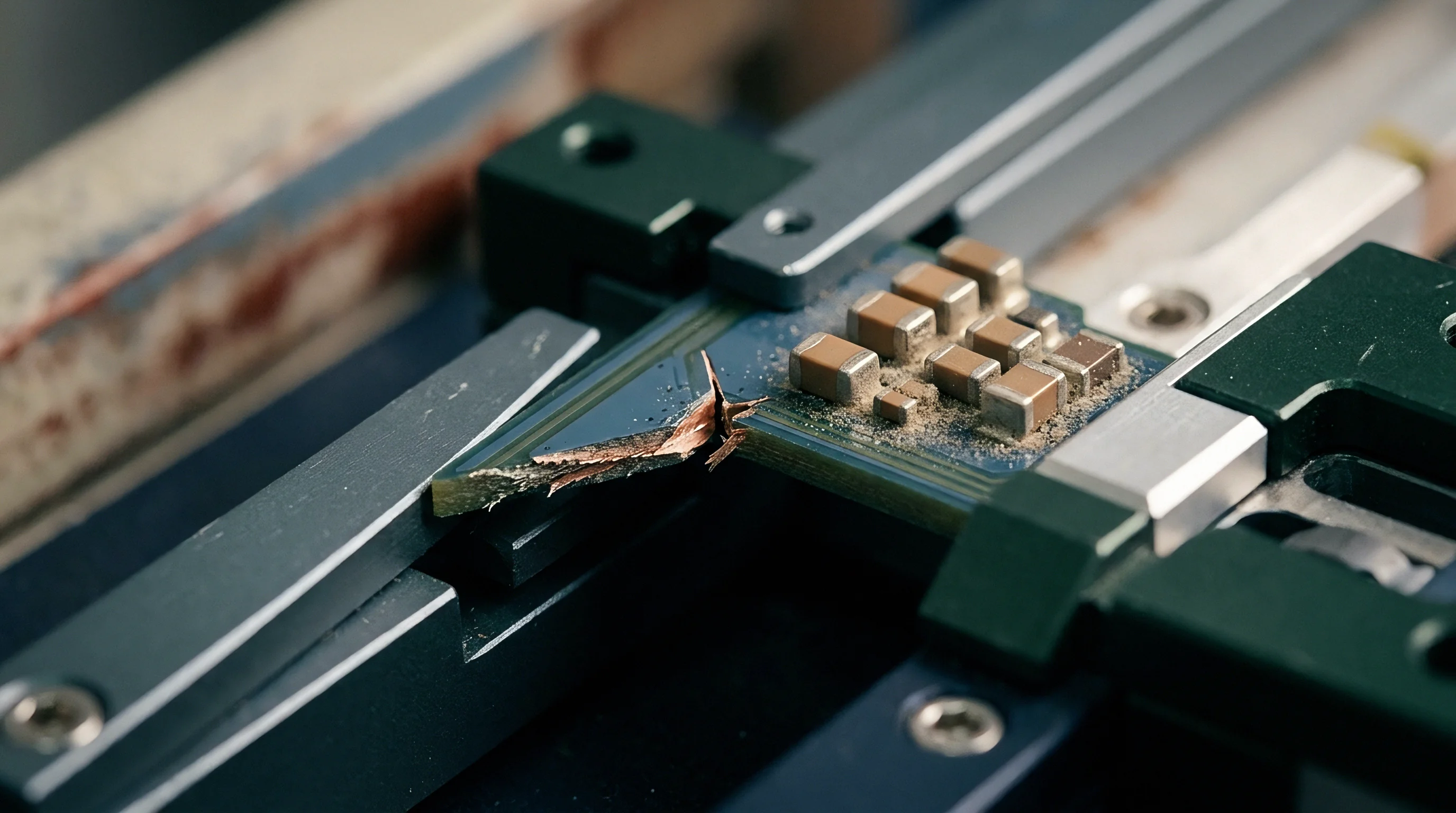
Soft breakdown establishes localized paths carrying micro-ampere leakage currents. Small as these currents are, they produce intense local Joule heating. That localized heat speeds up bond breaking in surrounding oxide, widening the conductive filament.
In high-power RF transistors, the jump from soft to hard breakdown happens fast. High RF voltage swings riding on top of DC bias dump energy right into the breakdown site. Once hard breakdown hits, gate current spikes to milliampere levels, clamping internal bias networks and permanently killing the transceiver.
| Mechanism | Physical Root Cause | Primary RF Circuit Affected | Measured Degradation Impact | Reversibility |
|---|---|---|---|---|
| NBTI | Si-H dissociation at pMOS gate oxide interface | Bias current mirrors & LNA gain stages | 1.2 dB LNA gain loss; 15% bias current drop | Partial (via thermal anneal) |
| PBTI | Electron trapping in oxygen vacancies (high-k) | Digital control logic & mixer switches | Switch RDS(on) increase by 22% | Partial (via zero-bias relaxation) |
| HCI | Hot carrier injection near drain junction | RF Power Amplifier output stages | 1.8 dBm drop in PA P1dB compression point | Irreversible |
| Soft TDDB | Percolation defect path formation across oxide | VCO varactor & resonator capacitors | 8 dB/Hz phase noise degradation at 10 kHz offset | Irreversible |
| Hard TDDB | Thermal breakdown filament melting dielectric | Gate oxide & inter-metal decoupling caps | Complete transceiver catastrophic short circuit | Irreversible |
Vetting module suppliers requires reviewing their TDDB reliability reports. Several red flags appear when assessing claims about long-term dielectric durability:
- Extrapolated Lifespan Oversimplification happens when suppliers fit accelerated TDDB data using linear voltage scaling instead of power-law models.
- Small Sample Size Bias shows up when Weibull shape parameters (β) are calculated from fewer than 30 test structures per wafer lot.
- Thermal Resistance Omission occurs when reports ignore self-heating in RF power transistors during continuous-wave bias stress testing.
- Decoupling Capacitor Neglect happens when suppliers qualify gate oxides but skip TDDB testing on BEOL metal-insulator-metal capacitors.
Foundries often argue that soft breakdown causes negligible shifts in digital logic ~ overlooking the fact that soft breakdown in analog RF blocks ruins receiver sensitivity long before digital gates stop working.


Damage
Wafer fabrication exposes delicate dielectrics to high-energy plasma during etching, deposition, and sputtering. Plasma-Induced Damage (PID) ~ often called the antenna effect ~ happens when conductive interconnect lines act as antennas, collecting electrostatic charge from the plasma. That accumulated charge forces tunneling currents through thin gate oxides, damaging the dielectric matrix before chips ever leave the fab.
Back-end-of-line processing adds mechanical stress on top of thermal and chemical damage. Chemical Mechanical Planarization (CMP) polishes oxide layers between metallization steps, but excessive down-force introduces micro-cracks into fragile low-k dielectrics, creating paths for moisture and metal ions to migrate later in manufacturing.
Plasma-Induced Charging and Antenna Effects during Processing
Plasma processing steps create non-uniform charge distributions across the wafer surface. Metal or polysilicon lines connected to gate oxides collect this charge, raising the gate electrode potential relative to the substrate. Once that potential exceeds the Fowler-Nordheim tunneling threshold, current flows straight through the thin gate dielectric.
Damage severity depends on the antenna ratio ~ the area of the metal conductor divided by the area of the thin gate oxide. Antenna ratios above 500:1 inject enough charge to form latent traps inside the dielectric matrix. While these latent traps don’t trigger immediate failures during wafer probing, they accelerate NBTI, HCI, and TDDB degradation during field operation, shortening device life by orders of magnitude.
Back-End-of-Line Interlevel Dielectric Degradation under RF Drives
BEOL interlevel dielectrics separate copper interconnect lines. To keep parasitic capacitance and signal crosstalk low in high-density layouts, foundries use porous ultra-low-k (ULK) dielectrics with dielectric constants (κ) below 2.5. However, porous ULK materials have lower mechanical strength, poorer thermal conductivity, and higher moisture sensitivity than standard silicon dioxide.
Under high RF voltage swings, intense electric fields between traces stress the porous low-k matrix. Copper ions migrate along pore walls to form conductive micro-paths, driving up inter-line leakage. At the same time, high RF power dissipation inside narrow copper traces creates localized heat; because ULK dielectrics dissipate heat poorly, hot spots form that accelerate dielectric breakdown.

Foundry Passivation Integrity and Environmental Moisture Ingress
The top passivation stack consists of silicon nitride (Si3N4) and silicon oxynitride layers that shield active circuitry from environmental contaminants. Silicon nitride acts as a reliable barrier against moisture and mobile alkali ions (Na+, K+).
Pinholes, micro-cracks, or high tensile stress in this layer ruin hermetic protection. Moisture penetrating the passivation reacts with underlying PECVD dielectrics, hydrolyzing siloxane bonds into polar hydroxyl groups (Si-OH). This water ingress boosts the dielectric constant, increases microwave loss tangent, and forms ionic conduction paths that speed up metal corrosion and dielectric breakdown.
Standard RFQ procurement terms mandate that foundries maintain maximum plasma antenna layout rules below 200:1 for all sensitive analog gate structures.
Preventing processing damage requires strict design rules and explicit wafer qualification terms in manufacturing contracts:
- Antenna Diode Protection mandates substrate grounding diodes next to long interconnect runs to divert plasma charges safely.
- Layout Dummy Fill Restrictions require dummy fill patterns that avoid floating conductive islands near high-frequency signal lines.
- Back-End Bake Verification requires post-CMP thermal bakes to drive off residual moisture before depositing final passivation.
- Passivation Stress Balancing mandates matched compressive and tensile stress layers in the Si3N4/SiON stack to prevent film cracking.
Contracts should explicitly state that any wafer lot exceeding antenna ratios of 200:1 without protective substrate diodes is subject to immediate rejection at the supplier’s expense.
Lifespan
Extrapolating dielectric lifespan from short-term lab data to multi-year field requirements is essential when selecting hardware components. Radio modules deployed in commercial, industrial, or utility infrastructure need to run reliably for 10 to 15 years under constant environmental and electrical stress. Predicting that operating life takes mathematical reliability modeling combined with realistic margins for link budget degradation.
Standard semiconductor qualification uses high-temperature operating life (HTOL) testing to accelerate wearout. By exposing devices to elevated temperatures (typically 125 to 150 degrees Celsius) and over-voltage conditions (1.2 to 1.5 times nominal supply), engineers compress years of field aging into weeks of lab testing.

Modelling Long-Term Reliability from Accelerated Lifetime Data
Mapping accelerated test results back to normal operating conditions relies on the Arrhenius-Eyring acceleration model. The acceleration factor (AF) accounts for both thermal and voltage acceleration:
AF = expleft( fracEakB left( frac1Tfield – frac1Tstress right) right) · expleft( γ left( Vstress – Vfield right) right)
Here Ea is the activation energy in electron-volts, kB is Boltzmann’s constant, Tfield and Tstress are temperatures in Kelvin, γ is the voltage acceleration factor, and Vstress and Vfield are the stress and field operating voltages.
Extracting accurate values for Ea and γ requires multi-cell testing across several temperature and voltage combinations. Relying on inaccurate acceleration parameters produces overly optimistic lifespan estimates, leaving deployments exposed to early field failures.

Radio Link Budget Degradation over Multi-Year Field Deployment
Dielectric degradation directly degrades the wireless link budget. Over a 10-year operating lifespan, cumulative gate oxide degradation in a transceiver lowers output power and degrades receiver sensitivity.
Take a sub-GHz radio link for smart utility metering running at 868 MHz. At deployment, the transceiver outputs +27 dBm with an LNA noise figure of 2.5 dB. Paired with 2 dBi omnidirectional antennas at both ends and using 50 kbps 2-FSK modulation (with a -106 dBm sensitivity threshold), the initial link budget works out to:
Link Budget = Ptx + Gtx + Grx – Psensitivity = 27 + 2 + 2 – (-106) = 137 dB
After 10 years of operation at an average ambient temperature of 55 degrees Celsius, dielectric wear takes its toll. HCI and NBTI in the power amplifier cause a 1.5 dB drop in Psat. At the same time, PBTI and interface trap growth in the LNA input raise the noise figure from 2.5 dB to 3.8 dB, degrading receiver sensitivity to -104.7 dBm.
Meanwhile, surface channel losses in the high-resistivity substrate add 0.8 dB of attenuation in the front-end switch.
The degraded link budget after 10 years equals:
Link Budget10yr = (27 – 1.5 – 0.8) + 2 + 2 – (-104.7) = 133.4 dB
That cumulative wear reduces total link budget by 3.6 dB. In an urban setting with a path loss exponent of 3.8, losing 3.6 dB of margin shrinks effective range by 24 percent. An IoT network built without accounting for dielectric aging will see node dropouts and packet loss as the hardware matures.
Designing wireless nodes with a mandatory 4 dB wearout fade margin ensures reliable connectivity over a 15-year operational lifespan despite dielectric performance decay.

Commercial Procurement Rules for Dielectric Reliability Guarantees
Managing reliability risks requires putting clear technical requirements directly into procurement contracts. Hardware buyers need to look beyond datasheet figures and insist on verified reliability dossiers from silicon vendors.
| Test Profile | Sample Size | Stress Voltage | Stress Temp | Duration | Pass/Fail Acceptance Criteria |
|---|---|---|---|---|---|
| HTOL Standard | 3 lots × 77 units | 1.2 × Vnom | 125 °C | 1000 hours | Zero catastrophic failures; Vth shift < 25 mV |
| HTOL Extended | 1 lot × 45 units | 1.3 × Vnom | 150 °C | 2000 hours | Pout degradation < 0.5 dB; NF shift < 0.5 dB |
| ESD Latent Stress | 1 lot × 30 units | 80% HBM Limit | 25 °C | 100 pulses | Gate leakage increase < 2× baseline |
| RF High-Power Burn-In | 2 lots × 50 units | Vnom at P3dB | 85 °C | 500 hours | Harmonic distortion increase < 3 dB |
Procurement contracts should require suppliers to share raw Weibull plot data for gate oxide TDDB, NBTI drift rates, and substrate trap density metrics for each primary fab facility. Securing second sources for critical RF SoCs prevents supply chain stalls if a primary foundry hits yield or reliability issues. High-reliability programs should also require silicon vendors to issue Process Change Notifications (PCN) at least 12 months before modifying gate dielectric deposition tools, oxidation furnace protocols, or passivation chemistry.
Quantifying dielectric wear rates helps engineering teams balance upfront hardware costs against long-term maintenance. Paying an extra 0.35 USD per module for a passivated trap-rich RF-SOI substrate built with high-k metal gate stacks can prevent expensive field recalls and keep link budgets intact across multi-decade deployments.