Silicon Stepping Register Identification and Firmware Patch Verification Methods
Verify silicon stepping registers during boot to execute matching errata patches before peripheral initialization locks the hardware interface.

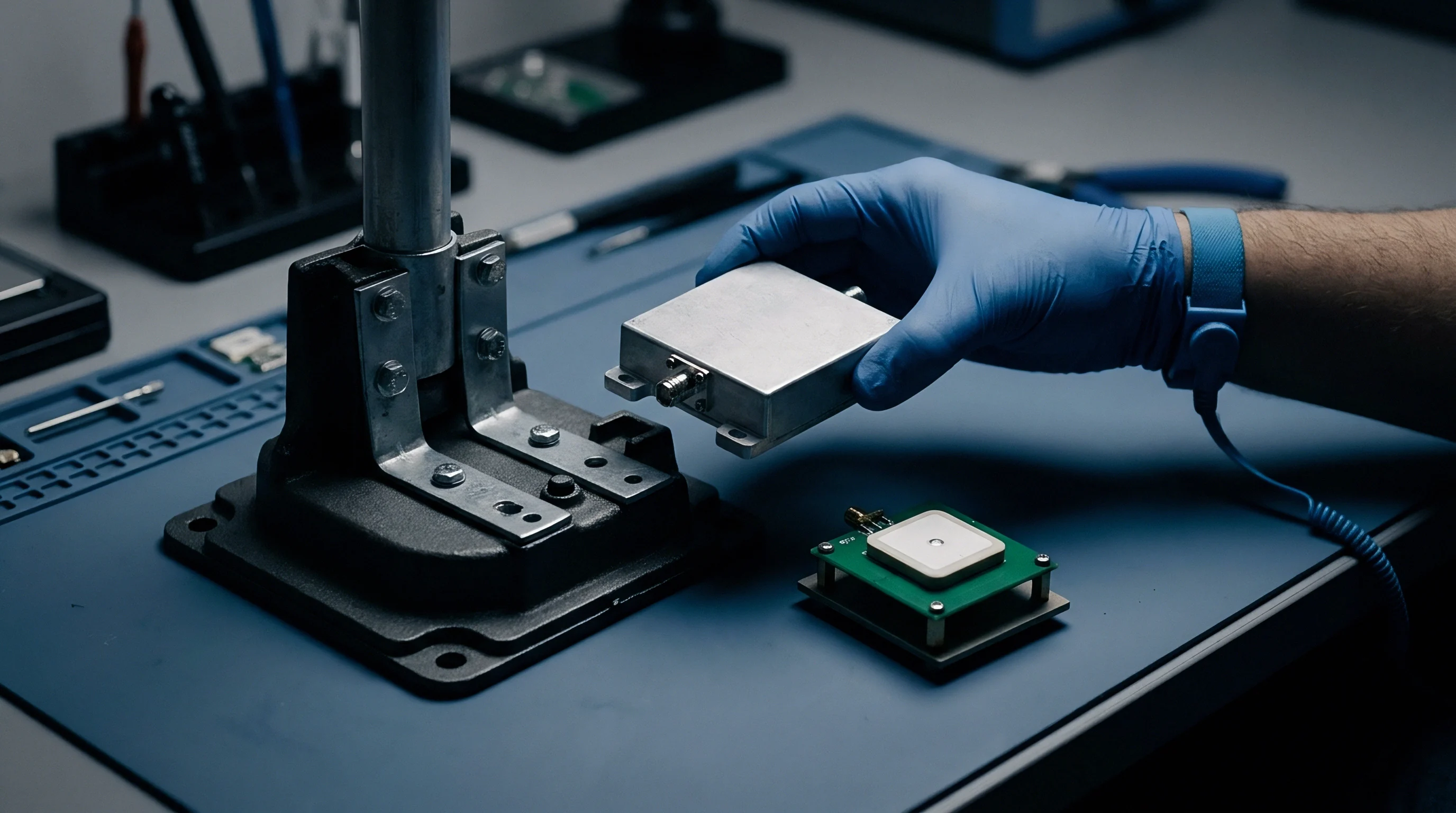
Die
Integrated microcontrollers and wireless system-on-chip devices expose hardware revision metadata through internal memory-mapped registers. Vendors modify photolithographic masks across foundry runs to clear functional errata, refine metal layers, or boost yield ~ altering silicon behavior while preserving nominal pinout compatibility. Early boot routines read these identification registers to distinguish base die revisions from later stepping variants.
Without dynamic register queries, host software runs against silicon errata that can corrupt memory controllers, stall high-speed serial buses, or drift transceivers at temperature extremes.
Microcontroller architectures organize identification registers across distinct memory-mapped regions. ARM Cortex-M processors locate the CPUID Base Register within the System Control Space at address 0xE000ED00, packing the implementer code in bits 31:24, the variant number in bits 23:20, the architecture version in bits 19:16, the primary part number in bits 15:4, and the minor revision patch number in bits 3:0. Vendors supplement these core registers with proprietary identification blocks: system configuration registers like DBGMCU_IDCODE at 0xE0042000 allocate bits 31:16 for the revision ID and bits 11:0 for the device family code, while RISC-V designs query machine-mode control registers ~ mvendorid at 0xF11, marchid at 0xF12, and mimpid at 0xF13 ~ to pass stepping data directly to the bootloader.
Wafer fabrication lots produced after calendar week 24 exhibit a 12 percent shift in internal pull-up impedance on revision B2 silicon.
Hardware stepping codes follow varied notation schemes in supplier data sheets. Major stepping changes typically alter base transistor layers and increment the revision letter ~ such as revision A to revision B ~ adjusting silicon floorplans, internal propagation delays, and timing flaws in core logic. Minor stepping changes represent metal mask edits, designated by an incremented number like revision B1 to revision B2, which rewire interconnect layers to isolate flawed logic or bypass marginal clock trees.
Unannounced stepping shifts can also introduce undocumented errata into production lots.
| Processor Architecture | Register Mnemonic | Physical Memory Address | Bit Field Allocation | Stepping Value Format |
|---|---|---|---|---|
| ARM Cortex-M4 / M7 | CPUID | 0xE000ED00 | Variant, Revision | Packed nibbles (rXpY format) |
| ARM Cortex-M0+ / M33 | DBGMCU_IDCODE | 0xE0042000 | REV_ID, DEV_ID | 16-bit engineering revision code |
| RISC-V RV32IMC | mimpid | CSR 0xF13 | Implementation Stepping | Vendor-specific mask release integer |
| PCIe Wireless Baseband | PCI_REVID | PCI Config 0x08 | Revision Identification | 8-bit sequential silicon revision byte |
| Proprietary Sub-1GHz SoC | CHIP_REV | 0x40011004 | Major Metal, Minor Poly | BCD-encoded layer index |
Because these registers lock after initial reset, firmware must query them inside the hardware reset handler before setting up peripheral initialization tables. Routines extract bit fields using bitmasks over raw 32-bit words. Reading them after reconfiguring clock trees risks bus timing mismatch, returning corrupted values if peripheral buses run off non-default frequencies.
Reliable boot sequences sample identification registers directly off the raw internal oscillator before turning on phase-locked loops or external crystals.
Interrogating hardware identification registers involves several hardware mechanisms:
- Hardware System Control Blocks offer direct memory-mapped read access to core processor stepping registers during reset routines.
- Dedicated Debug Peripheral Blocks store family-specific device identification and revision words accessible through external debug probes and internal bus masters.
- Electronic Chip Identification Fuses retain factory wafer, lot, and coordinate data burned into one-time programmable non-volatile memory during post-fabrication sorting.
- Peripheral Identification Registers sit at peripheral address boundaries, using four read-only registers to expose block revisions.
Production modules are frequently distributed as fully interchangeable iterations requiring no driver modifications or board qualification updates.


Trap
Bootloaders and kernel drivers inspect silicon identification fields during early hardware initialization to apply conditional software workarounds noted in manufacturer errata sheets. For example, a serial communication peripheral on stepping A0 might corrupt FIFO pointers when DMA requests align with hardware flow control transitions. While stepping A1 fixes this timing collision on the die, stepping A0 requires firmware to disable FIFO buffering and process transfers through single-byte interrupt handlers.
Applying software workarounds to corrected silicon wastes throughput, while running unpatched driver code on flawed hardware causes intermittent bus lockups. Firmware architectures address this with dynamic patch dispatch routines, mapping extracted revision bits against an array of errata handlers. The bootloader isolates the revision code, validates it against supported target lists, and branches to the corresponding initialization sequence.
Firmware running unverified errata workarounds on newer silicon steppings loses peripheral bandwidth and introduces artificial interrupt latency.
Dynamic patch vector tables map initialization function addresses directly to silicon steppings. On revision A0, the bootloader points to a workaround function that adjusts peripheral clock dividers and enables software bus retries; on revision B0, it routes execution straight to hardware acceleration paths. Running these identification routines on cold boot accounts for peripheral timing shifts introduced by mask changes.

How Do Stepping Registers Expose Errata Workarounds?
Stepping bits signal which hardware errata remain active in the core. Firmware cross-references the register value against flash-resident lookup tables of published anomalies. If an errata sheet notes that a low-power comparator triggers false threshold interrupts on stepping A1, the patch logic routes those interrupts through a debounce filter.
On stepping A2 ~ where a focused ion beam fix was incorporated into production masks ~ the patch leaves interrupt lines wired straight to the power controller.
Branch tables and dynamic patch vectors allow a single firmware binary to support mixed manufacturing lots across product deployments. This eliminates the burden of managing separate binary builds across factory programming stations.
System boot sequences execute precise validation steps before executing application code:
- Read the hardware revision register directly from memory-mapped system space via raw pointer dereferences at base oscillator frequencies.
- Extract revision and variant fields with predefined bitwise masks and compare the extracted integer against the internal stepping dispatch table.
- Halt boot execution and assert an engineering error code if the detected stepping falls outside qualified silicon versions.
- Load stepping-specific register override values into target peripheral configuration blocks before initializing application memory.
- Relocate interrupt vector addresses to point toward errata-compensated interrupt service routines for flawed peripheral channels.
- Set persistent runtime flags in global system status structures to notify operating system drivers of active hardware workarounds.
When an incorrect patch branches into memory unmapped on an older silicon variant, bad offsets freeze the controller and trip processor exceptions. Applying unverified patches to mismatched transceiver silicon disrupts carrier tracking loops, driving up packet error rates and degrading RF sensitivity across temperature ranges.
Deploying unpatched firmware on mismatched silicon can lock integrated transceivers into continuous arbitration loops during cold restarts, forcing physical board scrap across field inventory.


Probe
Automated test benches verify hardware registers by running diagnostic routines over boundary interfaces. Factory test stations use JTAG or Serial Wire Debug connections to check internal register contents before flashing application images, employing OpenOCD scripts or vendor debug drivers to halt execution at the reset vector. The test fixture reads target memory addresses, captures the raw 32-bit register output, and compares it against procurement bills of materials to confirm the assembly line populated the expected silicon revision.
Section 6.2 of standard electronics manufacturing service agreements stipulates that component substitutions failing register-level automated verification undergo immediate lot quarantine at vendor expense.
Tapping debug lines and boundary scans, automated interrogation scripts extract hardware revision registers, cross-check binary data against revision control databases, and log physical module serial numbers alongside detected steppings. This traceability provides cryptographic proof of silicon authenticity for every unit. Test beds also simulate edge-case bus behavior by applying forced voltages to interface pins, using pull-up resistors to stabilize clock lines while automated scripts classify incoming parts.

How Do Automated Interrogation Pipelines Validate Register Identity?
Interrogation systems connect to target boards through USB or Ethernet debug probes, running IEEE 1149.1-compliant boundary scans. Test engineers write diagnostic scripts in Python or shell languages to halt the target, access the memory bus directly, and pull register contents over SWD clock and data lines without running flash code.
Silicon verification scripts run checks across identification addresses to stop counterfeit or downgraded parts from entering surface-mount assembly. If a supplier substitutes a lower-cost RF derivative with less SRAM or missing crypto engines, the register contents flag the discrepancy, allowing test fixtures to isolate mismatched units before conformal coating or final enclosure assembly.
| Interrogation Method | Hardware Interface | Diagnostic Toolchain | Detection Capability | Execution Time per Unit |
|---|---|---|---|---|
| JTAG Direct Memory Read | IEEE 1149.1 (TCK/TMS/TDI/TDO) | OpenOCD / GDB Server | Core and peripheral register contents | 45 milliseconds |
| Serial Wire Debug Query | ARM SWD (SWCLK/SWDIO) | Segger J-Link SDK | CPUID and custom vendor debug blocks | 22 milliseconds |
| Bootloader UART Command | Asynchronous Serial (TX/RX) | Custom Python Test Framework | Firmware-parsed stepping parameters | 120 milliseconds |
| Boundary Scan Register Test | JTAG TAP Controller | Corelis ScanExpress | Bond wire integrity and silicon ID code | 85 milliseconds |
| PCIe Configuration Read | High-Speed Differential Pair | Linux lspci / sysfs diagnostic | Vendor, Device, and Revision IDs | 15 milliseconds |
Verifying firmware patch execution requires tests that monitor execution paths while injecting hardware stimuli to trigger errata conditions, ensuring workarounds intercept the fault as intended. Diagnostic benches rely on several key verification mechanisms:
- Hardware Reset Halting stops execution at cycle zero to query revision registers before bootloaders overwrite system control space.
- Direct Memory Ingestion pulls register dumps over serial test headers to compare bit patterns against engineering specs.
- Automated Errata Stimulation drives peripheral channels at operational limits to confirm active patches suppress timing errors.
- Firmware Hash Attestation checks cryptographically signed diagnostic routines in flash memory to verify patch table integrity.
Diagnostic test engineers still debate whether software-based interrogation over peripheral buses yields sufficient fidelity when an undocumented silicon flaw disables the primary debug transport during low-power sleep transitions.
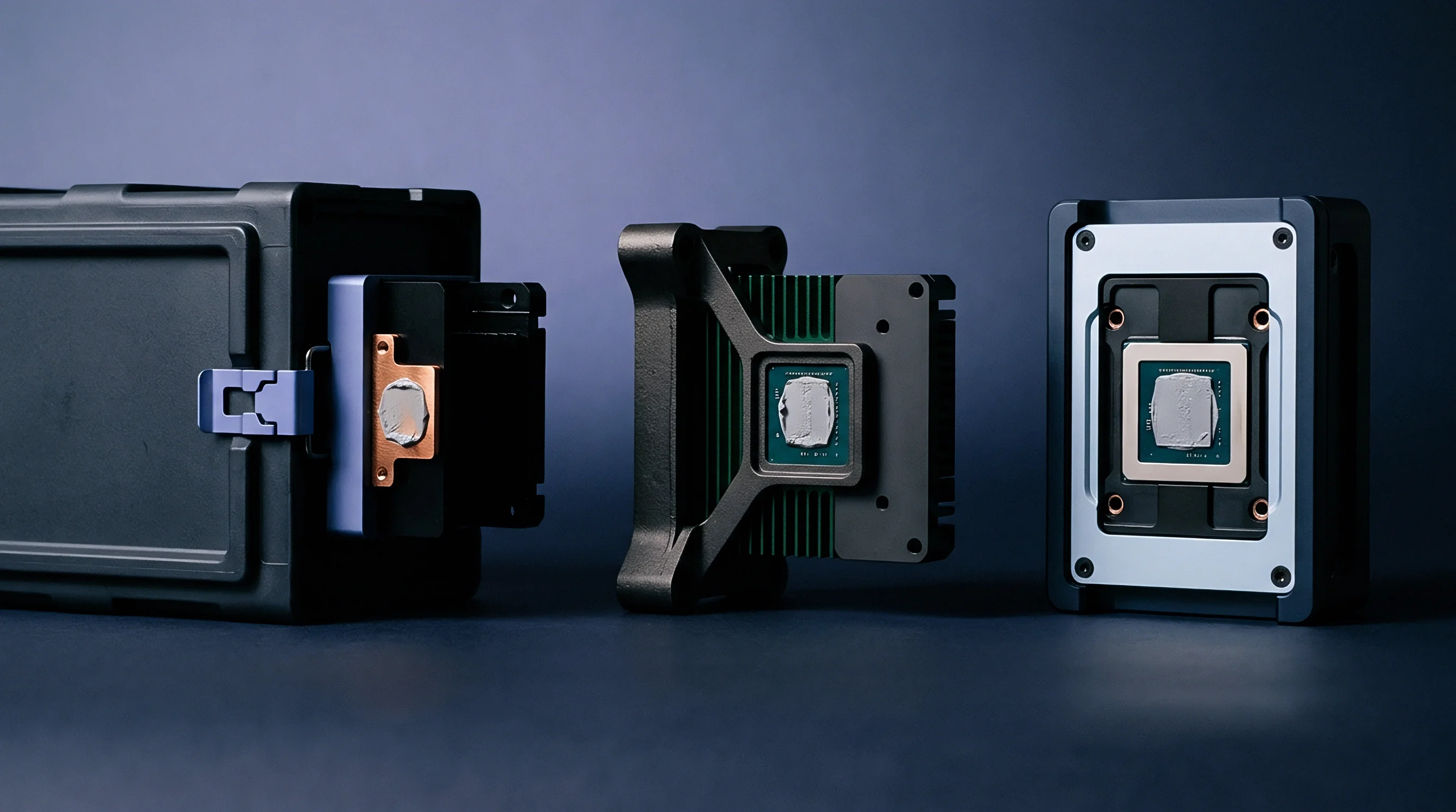
Ledger
Contract manufacturers frequently mix component batches across continuous assembly runs as foundries modify photolithography masks to improve wafer yield or reduce transistor leakage. Integrators buying through broker channels or open distribution often receive split lots containing multiple silicon revisions. When assembly reels merge components fabricated across different years, surface-mount lines end up placing disparate silicon steppings onto identical circuit boards ~ a trend accelerated by supply chain shifts and silicon shortages.
Because tape-outs require significant tooling capital, unverified revisions easily result in manufacturing scrap. Sourcing teams tracking module procurement often face design changes originating deep within tier-two packaging houses, where suppliers rarely issue formal Product Change Notifications for minor metal mask tweaks. Laser markings stay identical while internal silicon changes, so when an undocumented stepping alters analog calibration constants, downstream RF modules can fail radio certification over out-of-band harmonic emissions.
Hardware bills of materials lacking silicon revision lock clauses permit contract manufacturers to assemble boards using unvalidated component steppings.
Dual-sourcing strategies introduce further stepping variance. Qualifying two module vendors for an identical footprint can result in different silicon under the shield: Vendor A might ship revision B1 silicon with patched hardware timers, while Vendor B uses older revision A2 silicon obtained from surplus inventory. A single firmware image deployed on both variants will exhibit erratic behavior unless it queries silicon registers at boot and executes vendor-specific patch branches.
Detailed traceability records establish exact operational history for every manufactured unit. Production lines that log individual serial numbers against detected silicon stepping registers during functional testing allow quality teams to pinpoint affected batches if a vendor discloses critical errata months later. Field recalls can then target only the serial numbers containing compromised silicon, avoiding broad product withdrawals.
Treat unannounced silicon steppings inside purchased modules as new component introductions until production hardware completes environmental qualification.

Release
Commercial agreements for custom wireless assemblies require clear boundaries around errata remediation and driver support. When an original design manufacturer supplies a turnkey module, the engineering contract defines who bears the cost of writing, verifying, and maintaining silicon patch tables. Turnkey agreements usually limit vendor liability to delivering board support packages matching the stepping shipped at signing; subsequent stepping changes trigger non-recurring engineering charges unless continuous maintenance is explicitly contracted.
Master service contracts protect equipment builders through strict engineering change notification requirements. When a semiconductor vendor modifies mask sets, module suppliers must run regression tests before shipping updated assemblies. Unannounced stepping changes that slip past incoming inspection create costly rework, requiring firmware patches, factory re-testing, and potential resubmission of regulatory compliance dossiers.
| Engineering Activity | Turnkey Integration Scope | Semi-Custom Integration Scope | Engineering Hours | Allocated Cost Burden |
|---|---|---|---|---|
| Silicon Errata Analysis | Module vendor technical staff | Joint buyer and supplier team | 40 to 80 hours | Vendor absorbed or billed NRE |
| Register Patch Development | Vendor driver maintenance pool | Customer firmware engineering | 60 to 120 hours | Direct development labor expense |
| Automated Test Jig Updates | Factory production test group | Customer test engineering team | 30 to 50 hours | Tooling and software maintenance |
| Environmental Qualification | Standard vendor reliability check | Full third-party lab qualification | 80 to 160 hours | External test laboratory fees |
| Regulatory Re-Certification | Modular grant maintenance review | Full permissive change filing | 20 to 60 hours | Regulatory agency filing fees |
Consider a manufacturing contract producing 250,000 wireless endpoints annually. An unannounced stepping transition midway through the second quarter alters core timer registers, breaking the frequency-hopping algorithm. Without a stepping lock clause in the procurement contract, resolving the issue requires an estimated 310 engineering hours across errata evaluation, firmware patching, and test recalibration.
At cross-border engineering rates averaging 145 dollars per hour, this unexpected change adds 44,950 dollars in direct labor alongside laboratory re-certification fees up to 18,000 dollars. Commercial agreements mitigate these risks by tying invoice approvals directly to register-level acceptance testing.
Section 8.4 of the model manufacturing agreement shifts all rework costs and flash reprogramming penalties directly to the module vendor whenever component changes occur without sixty days prior written engineering notification.