Long Term Silicon Aging Effects on Microcontroller Internal Relaxation Oscillator Thermal Compensation Curves
Silicon aging distorts internal relaxation oscillator thermal compensation curves over time, requiring dynamic runtime recalibration to prevent network failure.


Wafer
Baseline silicon parameters set the boundaries for lifetime stability. Internal relaxation oscillators in modern low-power microcontrollers generate system clocks by charging and discharging a capacitor network through a temperature-compensated current source. Output frequency depends directly on bias current magnitude, dielectric capacitance, and the threshold voltage set by an internal bandgap reference.
Running these microcontrollers at elevated junction temperatures over multi-year spans causes gradual structural changes within the underlying CMOS oxide layers. These lattice-level shifts alter the physical parameters behind the oscillator’s time base, degrading timing accuracy long before structural failure occurs.
Negative Bias Temperature Instability is the dominant aging mechanism in PMOS transistors embedded within bandgap references and current mirror arrays. When p-channel MOSFETs experience negative gate-to-source bias at elevated temperatures, Si-H bonds at the silicon-silicon dioxide interface break apart. Hydrogen atoms diffuse away into the oxide matrix, leaving behind unpassivated silicon dangling bonds known as interface traps.
At the same time, positive charges get trapped within the bulk gate dielectric. This accumulation of interface traps and fixed oxide charge shifts threshold voltage toward more negative values, reducing the effective overdrive voltage of the PMOS devices. In a relaxation oscillator, PMOS current mirrors establish the primary charging current for the internal timing capacitor.
As threshold voltage increases in magnitude, that charging current drops, steadily pulling down the uncompensated frequency of the clock generator.
Positive Bias Temperature Instability affects NMOS devices, especially those utilizing high-k metal gate dielectric stacks. Trapped electron density inside the gate oxide layer accumulates over operational life, shifting the NMOS threshold voltage positive. In switching comparators that bound the relaxation oscillator’s charge and discharge ramp, this positive threshold voltage drift delays the switching point.
The comparator takes longer to detect when capacitor voltage reaches the upper reference threshold. That added propagation delay extends each oscillation cycle, producing a downward frequency shift that compounds the current mirror degradation caused by NBTI.
Sub-Threshold Drift Mechanics in Analog Bias Blocks
Analog bias networks inside relaxation oscillators rely on precise transconductance matching to keep temperature coefficients low. Proportional To Absolute Temperature current generators work alongside Complementary To Absolute Temperature bias networks to create a temperature-independent reference current. Evaluating relaxation oscillator architectures requires isolating bandgap reference drift to determine how individual bias branches age under elevated thermal stress.
Threshold voltage shifts do not happen uniformly across all transistors on the semiconductor substrate. Devices subjected to higher operational gate-to-source voltages age faster than adjacent low-voltage devices, introducing a dynamic imbalance across differential pairs in the bandgap core.
Hot Carrier Injection further degrades switching transistors in the oscillator’s discharge path. During high-frequency switching transitions, energetic electrons pick up enough kinetic energy from the channel electric field to cross the silicon-silicon dioxide energy barrier. Injected into the gate oxide, these hot carriers generate targeted damage near the drain junction of the switching transistors.
Hot carrier injection alters transconductance and raises sub-threshold leakage current. Higher sub-threshold leakage creates a secondary discharge path across the timing capacitor during the charging phase, flattening the ramp slope, altering the period calculation, and adding high-frequency phase noise to the clock output.
Comparator Gate-Oxide Trapping and Delay Skew
Comparator response time forms an integral term in the total relaxation oscillator period equation. The oscillation period equals the sum of physical capacitor charging time and the internal propagation delay of the sensing comparator logic. In high-frequency internal RC oscillators operating between 16 MHz and 48 MHz, comparator propagation delay accounts for up to fifteen percent of the total clock period.
As gate-oxide trapping extends comparator delay over five to ten years of continuous thermal exposure, that delay claims a larger fraction of the total cycle. Threshold voltages shift upward during stress, analog bias networks drift, and leakage currents alter charging ramp slopes.
Time-Dependent Dielectric Breakdown represents the long-term wear-out phase of thin gate oxides and integrated capacitor dielectrics. Prior to complete oxide rupture, localized soft breakdown events introduce micro-leakage channels through the dielectric layer. Integrated timing capacitors, constructed using Metal-Insulator-Metal or polysilicon-to-polysilicon layers, experience a gradual reduction in effective parallel resistance as defect densities grow.
Lower parallel resistance allows charge to leak off the timing capacitor during the charging ramp, taking the oscillator progressively longer to reach the comparator reference voltage and causing a permanent low-frequency shift in the baseline clock.
Uncompensated relaxation oscillators exhibit approximately 420 ppm clock drift after two thousand hours of thermal stress at 125 degrees Celsius.
Selecting microcontrollers with internal relaxation oscillators for timing-critical applications without accounting for silicon aging risks system failure under thermal stress. Cumulative wear across bandgap references, current mirrors, comparators, and capacitor dielectrics shifts physical timing parameters past what standard factory trim calibrations can correct. A system deployed in harsh industrial or automotive environments risks unrecoverable communications loss, corruption of synchronous serial interfaces, and timing failures across field networks once threshold voltage drift exceeds the initial guard-band allocations in the microcontroller’s internal compensation registers.

Shift
Thermal compensation curves configured during automated wafer probing rely on frequency values measured at discrete ambient temperatures. Manufacturing test systems record oscillator output at 25 degrees Celsius and an elevated temperature point like 85 or 125 degrees Celsius, writing these calibration values into non-volatile eFuse or Flash memory blocks. At boot, internal control logic reads these calibration coefficients and uses an onboard Proportional To Absolute Temperature sensor to dynamically select trim capacitor banks or adjust current bias Digital-to-Analog Converters.
This factory compensation model assumes that physical relationships between temperature, transistor transconductance, and reference voltages remain static throughout the operational life of the microcontroller.
Physical aging undermines that static compensation model. Because bandgap references, PTAT temperature sensors, and relaxation oscillator core circuits age at unequal rates, the offset and curvature parameters stored in memory during manufacturing diverge from the physical reality of aged silicon. The temperature sensor itself experiences threshold voltage drift, shifting its voltage output per degree Celsius over time.
When an aged microcontroller reads a specific voltage from its internal PTAT circuit, the lookup engine retrieves a trim code corresponding to the original factory state rather than current conditions, applying an incorrect compensation value to the clock logic.
Mathematical Decomposition of Aging-Induced Curve Distortion
Factory thermal compensation typically models oscillator frequency offset as a second-order polynomial function of temperature. The compensated frequency target uses trim codes to adjust both the linear temperature coefficient and the quadratic curvature parameter. Over time, thermal compensation lookup tables degrade non-linearly as physical drift components evolve across operational time:
f_actual(T, t) = f_0(T_0) + Delta_aging(T, t)
In this relationship, f_0(T_0) represents baseline nominal frequency at room temperature, while alpha(t) and beta(t) represent time-dependent temperature coefficients that evolve as NBTI, PBTI, and HCI degrade the silicon junctions. The term Delta_aging(T, t) captures non-uniform frequency offset caused by localized oxide trap buildup. Because Delta_aging exhibits strong non-linear temperature dependence, an oscillator aged at 105 degrees Celsius demonstrates a vastly different error profile when operated back down at room temperature than an unaged device.
| Sub-Block Circuitry | Dominant Aging Mechanism | Physical Degradation Mode | Uncompensated Drift Direction | Impact on Thermal Compensation Curve |
|---|---|---|---|---|
| Bandgap Voltage Reference | PMOS NBTI / Resistor Drift | Threshold voltage shift in differential pairs | Negative frequency shift | Vertical offset shift across all temperatures |
| PTAT Temperature Sensor | NMOS PBTI / Junction Leakage | Sensitivity drift in mV per degree Celsius | Indirect error via trim selection | Horizontal temperature mapping error |
| Oscillator Comparator Core | Gate-Oxide Hot Carrier Trapping | Propagation delay increase | Negative frequency shift | Linear temperature slope distortion |
| MOM / MIM Capacitor Bank | Time-Dependent Dielectric Breakdown | Dielectric charge trapping and leakage | Positive or negative shift | Quadratic curvature parameter distortion |
| Bias Current Mirror DAC | Channel Length Modulation Drift | Transconductance mismatch in DAC legs | Gain error in current steps | Non-linear step discontinuity in trim levels |
The interaction between PTAT temperature sensor sensitivity drift and oscillator core frequency degradation creates a compound timing error. Consider an integrated PTAT sensor that exhibits a three percent decrease in output slope voltage after 10,000 hours at 105 degrees Celsius. At an actual die temperature of 105 degrees Celsius, the sensor outputs a voltage corresponding to 98 degrees Celsius based on its original factory calibration table.
The microcontroller compensation logic accesses the trim lookup table and applies a trim bit setting optimized for 98 degrees Celsius. However, the oscillator core has simultaneously undergone NBTI-induced frequency reduction requiring a stronger compensation trim word. The combination of under-reporting actual junction temperature and applying a degraded trim current results in a compound clock offset that easily exceeds protocol timing allocations.
Worked Example of Thermal Polynomial Failure
To quantify the breakdown of factory calibration, evaluate a 32 MHz relaxation oscillator using a second-order polynomial compensation system. Factory calibration sets the baseline trim at 25 degrees Celsius and programs a linear coefficient of 12.5 ppm per degree Celsius alongside a quadratic coefficient of -0.04 ppm per degree Celsius squared. At initial deployment, the microcontroller holds frequency stability within +/- 50 ppm across the full industrial temperature range of -40 degrees Celsius to +105 degrees Celsius.
After five years of continuous operation at an elevated ambient temperature of 105 degrees Celsius, bandgap degradation introduces a static offset shift of -180 ppm across all temperatures. Simultaneously, PMOS trap accumulation alters the linear temperature coefficient from 12.5 ppm per degree Celsius to 18.2 ppm per degree Celsius, while PTAT sensor drift adds a secondary horizontal mapping error equivalent to an 8 degrees Celsius temperature reading deficit at high thermal extremes. Evaluating the mathematical model at 105 degrees Celsius reveals the extent of the compensation failure:
Delta_f_total = Delta_f_offset + Delta_f_linear + Delta_f_quadratic
Substituting the aged system parameters into the error formulation yields:
Delta_f_total = -180 ppm + (18.2 ppm/°C × 88°C) + (-0.04 ppm/°C² × 88°C²)
Delta_f_total = -180 ppm + 1103.04 ppm – 744.0 ppm
Delta_f_total = +179.04 ppm error relative to target frequency.
The net clock frequency error at 105 degrees Celsius reaches +179.04 ppm from compensation misallocation alone, compounding with the baseline -180 ppm structural bandgap shift to produce an aggregate system error of -0.96 ppm at 105 degrees Celsius. However, when the thermal profile cycles back down to -40 degrees Celsius, unscaled compensation generates a massive uncorrected frequency overshoot exceeding +620 ppm, completely invalidating the product’s specification sheet tolerances.
Internal relaxation oscillator drift claims apply exclusively to unaged silicon tested immediately following factory trim execution.
Internal relaxation oscillators are characterized across temperature during qualification, but published datasheet parameters reflect initial performance directly after factory trimming. Long-term environmental drift falls under unrated end-of-life relaxation allowances rather than guaranteed thermal curve tracking specifications. Applications requiring sub-percent timing stability over extended service lives require external quartz crystal resonators rather than sole reliance on internal compensated RC oscillator blocks.

Margin
Timing margins shrink under thermal cycling. Radio frequency protocol stacks rely heavily on predictable microcontroller clock sources to establish precise sleep intervals, frame timing synchronization, symbol modulation rates, and packet correlation windows. When silicon aging alters the thermal compensation performance of an internal relaxation oscillator, the physical link layer of the radio transceiver suffers direct degradation.
In crystal-less wireless architectures, where the internal RC oscillator drives both the digital core and baseband timing logic, aging-induced frequency drift compresses the link budget, increases packet error rates, and degrades total network throughput.
Bluetooth Low Energy protocols place strict tolerances on Sleep Clock Accuracy. A BLE peripheral node enters deep sleep modes between advertising or connection events to conserve battery power, relying on its low-power sleep clock to drive the wake-up timer. The standard specification bounds allowable sleep clock uncertainty between +/- 20 ppm and +/- 500 ppm depending on configured connection parameters.
When central and peripheral devices schedule a connection event, both units calculate an active receiver window anchor point. The peripheral wakes up slightly early to account for potential clock drift, opening its receiver window for a duration proportional to its declared Sleep Clock Accuracy rating.
If aging shifts the internal relaxation oscillator driving the sleep timer beyond its Sleep Clock Accuracy allocation, the peripheral opens its receiver window too late or closes it before central transmission finishes. The peripheral fails to capture the incoming packet preamble, causing connection event failures and triggering automatic retransmissions. To maintain connectivity, the BLE stack widens the receiver window during each anchor point, extending the active power dissipation period of the radio front-end.
Current consumption jumps from microampere baseline levels up to full active receiver drain, rapidly exhausting primary cell batteries in deployed asset trackers and industrial sensors.
Sub-GHz Protocol Frame Misalignment and Window Jitter
Sub-GHz long-range protocols, such as LoRaWAN and IEEE 802.15.4g, operate over extended distances where link margins are tightly optimized. In crystal-less LoRaWAN endpoint designs, internal relaxation oscillators drive the time base for Channel Activity Detection and Class A receive window timing. Class A end-devices open two precise receive windows, RX1 and RX2, at exact intervals following an uplink transmission, typically set to one second and two seconds respectively.
Current references define total timing jitter, and packet correlation windows require strict bounds.
Frequency drift in the microcontroller’s thermal compensation logic alters these receive window delays. If the internal oscillator drifts by more than 0.5 percent due to high-temperature silicon aging, the start of the RX1 window shifts by several milliseconds. The LoRaWAN gateway transmits the downlink frame at the precise scheduled timestamp, but the aged end-device opens its receiver out of frame alignment.
The spread-spectrum preamble fails to correlate, resulting in a dropped downlink packet. The end-device misses network MAC commands, downlink acknowledgments, and data payloads, forcing the protocol stack into power-hungry join-rejoin sequences that further accelerate system degradation.
| Wireless Standard | Critical Timing Parameter | Max Allowable Timing Error | Primary Protocol Failure Mode | System Operational Consequence |
|---|---|---|---|---|
| Bluetooth Low Energy | Sleep Clock Accuracy (SCA) | +/- 500 ppm (Configured) | Anchor point offset timing loss | Receiver window expansion, battery drain |
| LoRaWAN Class A | RX1 / RX2 Receive Window Delay | +/- 15 milliseconds | Downlink preamble correlation failure | Total downlink packet loss, network disconnection |
| IEEE 802.15.4 (Zigbee) | Symbol Duration / Mac Framing | +/- 40 ppm | Inter-frame spacing corruption | Acknowledge timeout, packet retransmissions |
| CAN-FD Industrial Bus | Nominal / Data Phase Bit Time | +/- 0.5 percent (+/- 5000 ppm) | Sample point bit misalignment | Bus error frame accumulation, bus-off state |
| Asynchronous UART | Baud Rate Bit Sampling | +/- 2.5 percent (+/- 25000 ppm) | Framing error on stop bit detection | Serial data corruption, telemetry loss |
Industrial communication interfaces experience similar breakdowns under thermal compensation aging. Controller Area Network and CAN Flexible Data Rate protocols demand tight clock synchronization across distributed node networks to establish bit-arbitration mechanics. CAN-FD data phases operating at rates up to 5 Mbps assign sampling points within small fractions of a bit period.
An internal relaxation oscillator that shifts outside the +/- 0.5 percent window across operating temperature causes local bit-sampling errors. Node controllers flag bit-stuffing errors, continuously incrementing internal transmit and receive error counters until the microcontroller enters a bus-off condition, severing communications with industrial control systems.
Field Failure Modes in Wireless Endpoints
Field installations reveal distinct failure signatures when microcontroller relaxation oscillators undergo long-term thermal compensation drift. These operational modes demonstrate how analog aging degrades system-level performance across field deployments:
- Progressive Sleep Window Expansion forces BLE sensor nodes to hold receiver circuits active for extended durations, increasing sleep state power consumption by up to four hundred percent and terminating battery service life prematurely.
- Asymmetric Downlink Packet Drop Rates occur in long-range sub-GHz radios where uplink transmissions succeed due to transmitter-initiated preambles, but scheduled downlink reception fails completely due to localized RX window time-skews.
- Thermal Cycling Connection Loss manifests when field nodes operate reliably during cool nighttime ambient conditions but experience complete network disconnection as sunlight raises internal enclosure temperatures to levels where aged compensation polynomial curves fail.
- Serial Communications Framing Corruption breaks local microcontroller-to-modem interfaces, generating unrecoverable asynchronous receiver-transmitter stop-bit errors that block modem configuration AT commands.
Sleep current calculations rely on static accuracy assumptions, while preamble detection demands sub-percent frequency alignment. Near operational boundaries, frame error rates spike exponentially. Field failures in wireless modules from high-temperature installations consistently show that microcontrollers using uncalibrated internal RC timing sources suffer severe receiver sensitivity degradation directly caused by timing window misalignments.
Standard industrial supply agreements stipulate that clock stability parameters apply only when microcontrollers operate within initial factory thermal specification envelopes.
Does the industry require a fundamental overhaul of standard micro-controller qualification protocols to account for the dynamic coupling between continuous high-temperature silicon aging and internal oscillator thermal compensation drift?

Screen
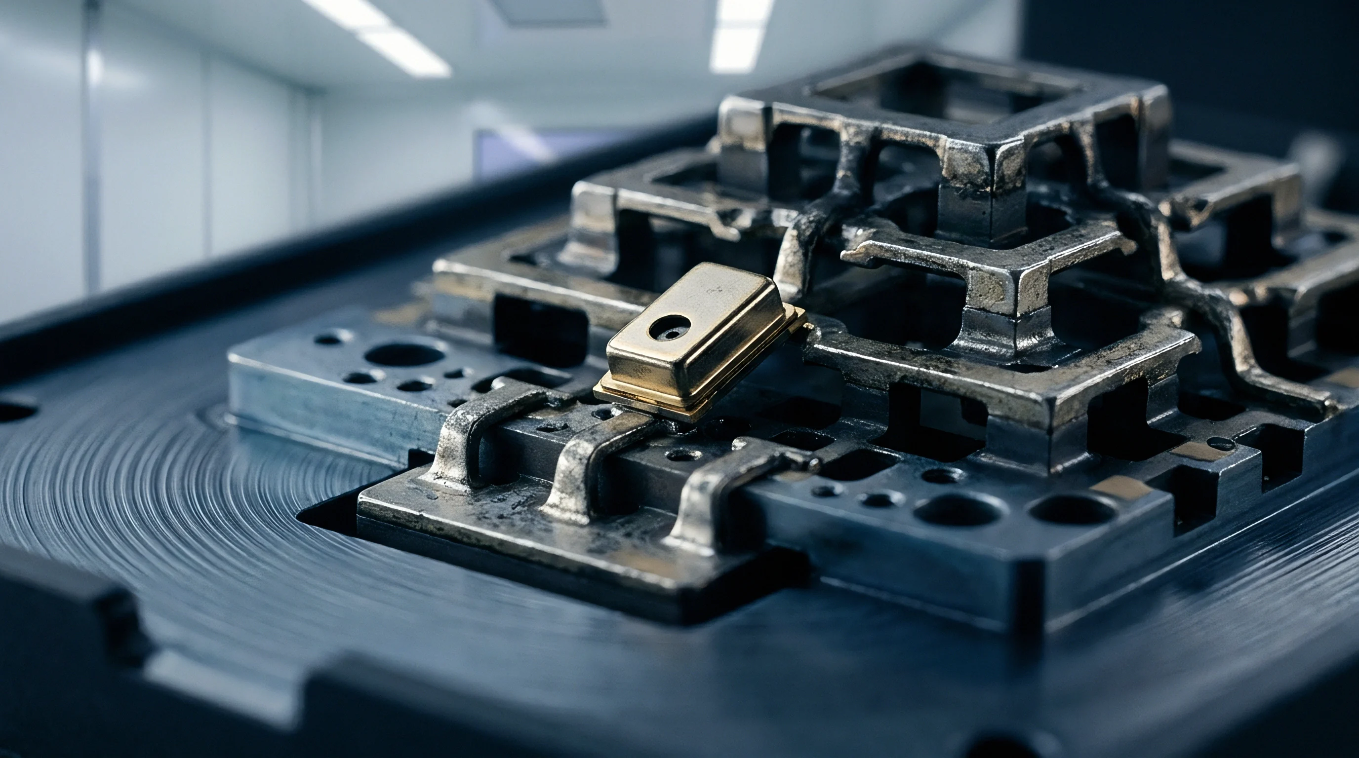
Accelerated life testing evaluates silicon endurance by subjecting integrated circuits to elevated temperatures and supply voltages well beyond standard operating conditions. High Temperature Operating Life qualification standards, defined under JESD22-A108 and AEC-Q100 guidelines, specify sample sizes, stress durations, and stress temperatures designed to simulate a ten-year operational life. Microcontroller qualification programs mandate stress testing at 125 degrees Celsius or 150 degrees Celsius for 1,000 hours.
However, standard production screening procedures focus heavily on pass-fail digital logic testing and static functional verification, frequently overlooking the slow, continuous drift of internal analog relaxation oscillator thermal compensation curves.
The physics of accelerated aging are modeled using the Arrhenius relationship to determine the Acceleration Factor for thermal stress. The model calculates how time-to-failure or degradation rate scales as a function of absolute temperature and activation energy:
AF = exp
In this expression, E_a represents the thermodynamic activation energy associated with a specific dielectric degradation mechanism, k represents Boltzmann’s constant (8.617 x 10^-5 eV per Kelvin), T_use represents the normal operational junction temperature in Kelvin, and T_stress represents the elevated qualification test temperature in Kelvin. For Negative Bias Temperature Instability and oxide trapping mechanisms in modern CMOS process nodes, activation energies generally range between 0.6 eV and 0.8 eV.
Using an average activation energy of 0.7 eV, exposing a microcontroller to 1,000 hours at 125 degrees Celsius (398.15 K) accelerates aging equivalent to operating the device at a continuous industrial ambient temperature of 55 degrees Celsius (328.15 K) for approximately 38,000 hours, or roughly 4.3 years. However, if the final deployment subjects the microcontroller to continuous junction temperatures of 85 degrees Celsius (358.15 K), that same 1,000-hour 125 degrees Celsius qualification test provides an equivalent operational duration of only 9,100 hours ~ slightly over one single year of real-world service life. Standard qualification time-frames fail to adequately model long-life industrial and automotive applications expected to remain operational for fifteen to twenty years.

How Can Qualification Screening Isolate Long Term Relaxation Oscillator Drift?
Detecting thermal compensation drift during volume production screening requires specialized test methodology integrated into standard Automated Test Equipment programs. Screening must isolate individual drift contributions from the internal bandgap reference, the PTAT temperature sensor, and the relaxation oscillator core. Relying solely on a single room-temperature frequency measurement during final test yields zero visibility into how the thermal compensation polynomial curve will evolve over years of high-temperature field service.
- Mount sample devices from wafer lots on high-precision temperature-controlled thermal chucks within automated testing handlers to establish baseline frequency measurements across three discrete thermal calibration points (-40 degrees Celsius, +25 degrees Celsius, and +125 degrees Celsius).
- Apply continuous high-voltage electrical stress to internal bias networks and integrated relaxation oscillator circuits while maintaining maximum rated junction temperatures for an initial 168-hour burn-in phase.
- Execute post-burn-in frequency characterization across the same thermal points, calculating the delta offset drift, linear temperature coefficient change, and PTAT mapping error for each device under test.
- Extract mechanism-specific drift parameters by fitting measured post-stress frequency outputs against the original factory eFuse compensation polynomial coefficients stored in non-volatile memory.
- Reject wafer lots exhibiting statistical drift values that exceed pre-calculated thermal compensation guard-bands, ensuring that only silicon displaying predictable NBTI and PBTI stabilization profiles enters high-reliability production supply chains.
High temperatures accelerate threshold voltage recovery, while guard bands prevent premature field failures. When devices undergo thermal stress during screening, removing the stress voltage and cooling the parts to room temperature initiates a partial recovery phase. Interface traps generated by NBTI re-passivate over time if hydrogen atoms diffuse back to the silicon-dioxide interface.
Test engineers must execute post-stress frequency measurements within strict time limits following thermal stress extraction to prevent recovery phenomena from masking operational aging drift.
eFuse array burn integrity introduces another screening vulnerability. Factory thermal compensation trim codes stored in one-time programmable eFuse structures rely on polysilicon or metal link rupture mechanics. Incomplete eFuse programming or post-stress charge migration within adjacent unburned fuse cells can corrupt stored calibration bits.
A single bit-flip in an eFuse thermal trim register alters compensation lookup logic, creating an instantaneous, discrete frequency step error that operates independently of transistor aging physics.
Per ISO 26262 functional safety audit frameworks, semiconductor manufacturers must document all analog clock drift mechanisms capable of violating system timing safety goals.
Standard procurement contract indemnification clauses explicitly state that semiconductor suppliers warrant product operation only to the bounds published within official datasheet electrical specifications at delivery. If a customer application fails in the field due to internal relaxation oscillator frequency drift after three years of operation at continuous elevated temperatures, legal liability rests entirely on the system integrator, provided the silicon vendor can demonstrate compliance with standard AEC-Q100 or JESD47 qualification testing protocols during initial lot release.

Remedy
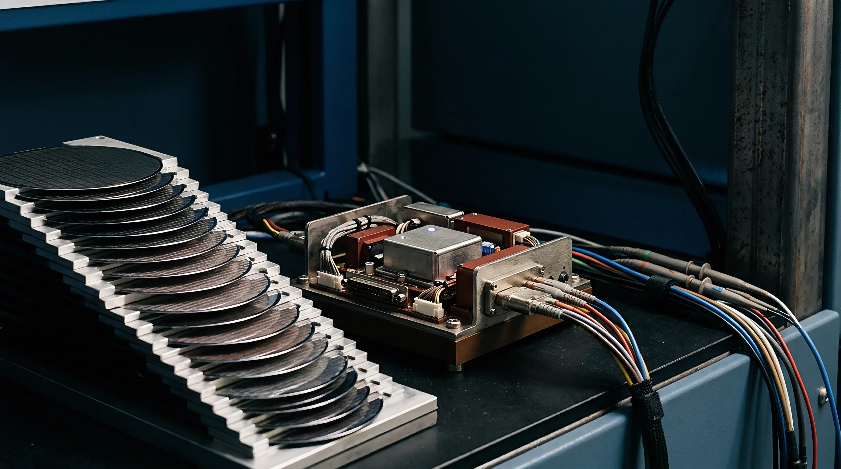
Field recalibration can restore baseline precision in systems subject to silicon aging. Embedded designers facing thermal drift in microcontroller relaxation oscillators need active architectural defenses. Relying on static, factory-programmed thermal compensation lookup tables for devices operating beyond five years at elevated junction temperatures inevitably leads to field degradation.
Mitigating clock compensation failure demands dynamic runtime firmware recalibration, hybrid dual-clock system architectures, external reference synchronization, and strict guard-band design methodologies.
Network-assisted dynamic recalibration offers an effective software-driven defense for connected endpoints. Modern wireless transceivers regularly receive time-stamped synchronization frames, preambles, or beacon headers from network infrastructure nodes such as cellular base stations, gateway routers, or central BLE controllers. System firmware can capture the arrival time of these external frames using high-speed hardware timer-capture channels clocked by the internal relaxation oscillator.
By comparing measured frame duration against the mathematically exact frame duration defined by the wireless standard, the microcontroller calculates its real-time internal oscillator frequency error.
Once the firmware calculates the precise frequency offset, it executes an internal trim update routine. The microcontroller writes an updated trim code to its dynamic clock control registers, overriding the stale factory eFuse thermal compensation value. This dynamic recalibration process automatically corrects for NBTI threshold voltage shifts, bandgap reference offset drift, comparator delay changes, and PTAT temperature sensor aging simultaneously.
Because recalibration relies on an external, highly stable radio frequency time base, the system continuously tracks aging degradation across the operational lifespan of the device.
| Mitration Strategy | Implementation Layer | Hardware Requirements | Power Budget Impact | Recalibration Precision |
|---|---|---|---|---|
| Network Frame Preamble Capture | Embedded Firmware | Radio transceiver, capture timer | Negligible (Uses existing RX frames) | High (+/- 10 ppm to +/- 50 ppm) |
| Dual-Temperature Flash Trim Update | System Application Logic | Internal Flash sector, PTAT ADC | Low (Periodic Flash write cycles) | Moderate (+/- 100 ppm) |
| Hybrid External Low-Power Crystal | Board Hardware Design | 32.768 kHz tuning-fork crystal | Very Low (Continuous microamp drain) | Very High (+/- 20 ppm over lifetime) |
| Mains Power Zero-Cross Timing | System Firmware | Optocoupler / Zero-cross circuit | Low (Continuous AC sensing) | High (Tied to grid stability) |
| Dynamic eFuse Bit Re-Mapping | MCU Bootloader Logic | Re-writeable eFuse / EEPROM block | Negligible (Executes at boot) | Moderate (+/- 150 ppm) |
Hardware-assisted hybrid clock topologies eliminate reliance on internal thermal compensation curves for timing-critical operations while retaining low power consumption. Integrating an inexpensive external 32.768 kHz tuning-fork quartz crystal resonator provides a stable, low-frequency time base. The internal high-frequency relaxation oscillator remains powered down during sleep states.
Upon wake-up, an internal Frequency Locked Loop uses the active 32.768 kHz crystal output to continuously measure and discipline the high-frequency internal RC oscillator, locking its output frequency to the external crystal reference before initiating baseband processing or serial communications.
Design Rules for Long-Life Embedded Architectures
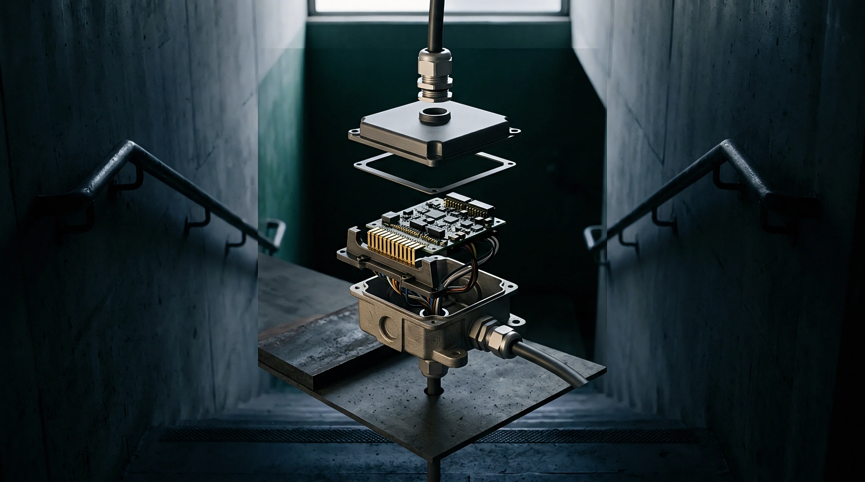
Engineers specifying microcontrollers for long-life deployments under thermal stress must enforce rigorous hardware and firmware design principles to guarantee timing stability over the product lifecycle:
- Protocol Receiver Window Guard-Banding must incorporate cumulative ten-year silicon aging drift allowances directly into software timing window calculations, expanding default BLE or sub-GHz receive window parameters by at least three hundred percent.
- Periodic Runtime Thermal Re-Trimming demands that firmware monitor internal PTAT temperature sensor deltas, executing dynamic trim register updates whenever system junction temperature changes by more than five degrees Celsius.
- Asynchronous Baud Rate Oversampling compels serial communications drivers to utilize maximum available hardware oversampling ratios, selecting 16x oversampling modes over 8x modes to maximize bit-sampling tolerance margins.
- Voltage Regulator Guard-Banding requires internal low-dropout regulators driving analog relaxation oscillator blocks to maintain output voltage ripple below five millivolts across all operating temperature extremes.
In high-reliability embedded system design, an internal relaxation oscillator should never serve as the sole timing reference for synchronous communications protocols unless the system incorporates automatic runtime self-calibration capable of tracking lifetime silicon degradation.