Meaning
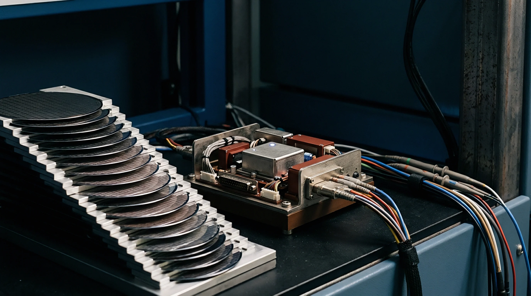
Wafer technology utilizes a high resistivity base and a thin insulating layer to optimize the performance of high frequency circuits. In the production of cellular front-end modules, rf-soi enables the integration of switches and power amplifiers on a single die. This architecture reduces the parasitic capacitance that otherwise limits the speed of standard bulk silicon devices.
Signal Isolation
Electromagnetic coupling between adjacent components is minimized by the presence of the buried oxide layer. This barrier prevents signal leakage into the substrate, which is a common problem in traditional designs.
Harmonic Distortion
Nonlinear effects in the substrate can generate unwanted interference that disrupts wireless communication. The high resistivity of the silicon base reduces these distortions by preventing the formation of a parasitic conduction layer. Integrating a trap-rich layer at the interface further improves linearity by immobilizing free charges that would otherwise respond to the radio frequency field.
This combination of layers allows for the creation of high-linearity devices that are required for advanced communication standards.
Integration Level
Modern smartphones use this technology to combine several radio functions into a compact package. This consolidation reduces the total footprint of the radio assembly and lowers the overall power consumption. Manufacturers prefer this substrate because it supports the complex requirements of 5G networks while maintaining a manageable production cost.