
Trap Rich Layer Physics for RF Silicon Substrates
Trap-rich polysilicon layers beneath buried oxide pin interface carriers to eliminate parasitic conduction and lower sub-6 GHz harmonic generation.
Trap-rich polysilicon layers beneath buried oxide pin interface carriers to eliminate parasitic conduction and lower sub-6 GHz harmonic generation.
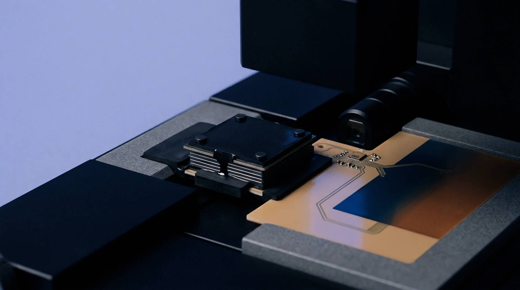
Trap-rich polysilicon layers suppress parasitic surface conduction in high-resistivity silicon transceivers, lowering second harmonics below -85 dBc at +25 dBm RF input.
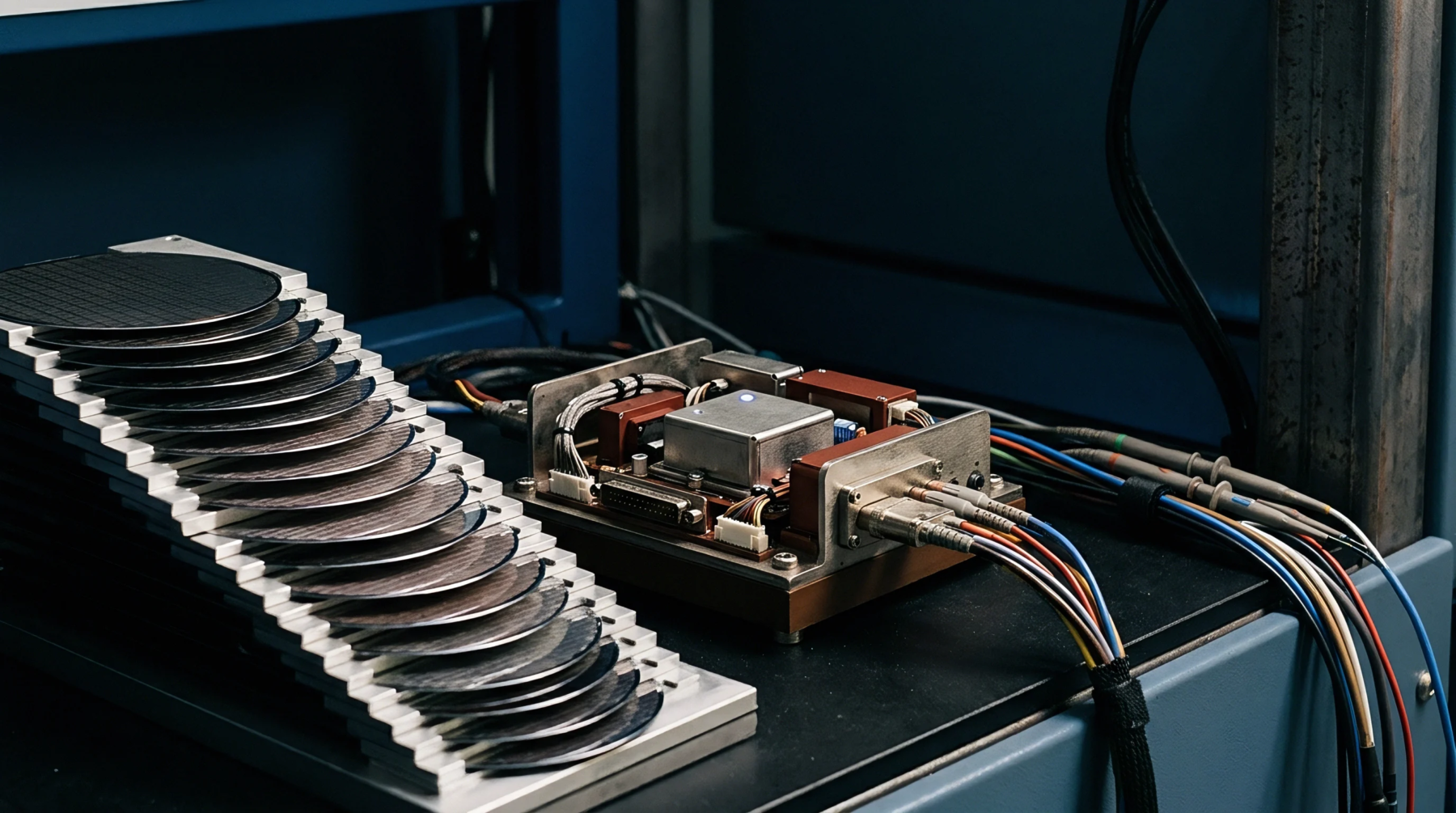
Dielectric breakdown modeling on trap rich silicon requires temperature adjusted voltage acceleration factors to prevent early RF switch gate oxide failure.

Trap-rich polysilicon passivation pins interface charges on high-resistivity silicon, suppressing surface conduction and harmonic spur spikes across RF switches.
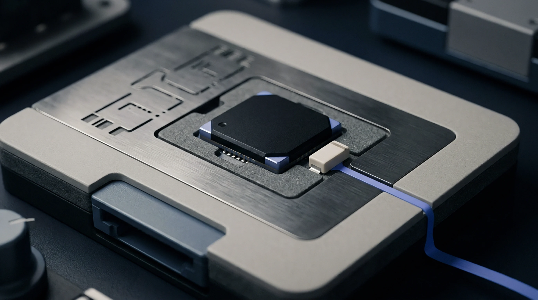
Substrate dielectric degradation reduces RF transceiver link budgets over time, requiring a minimum four-decibel margin allowance during module procurement.
Expertise is a utility, not a secret. sentiention™ publishes its working knowledge as open reference: intelligence layer covering the materials it sources, the markets it enters, and the reference that serves both.