Meaning
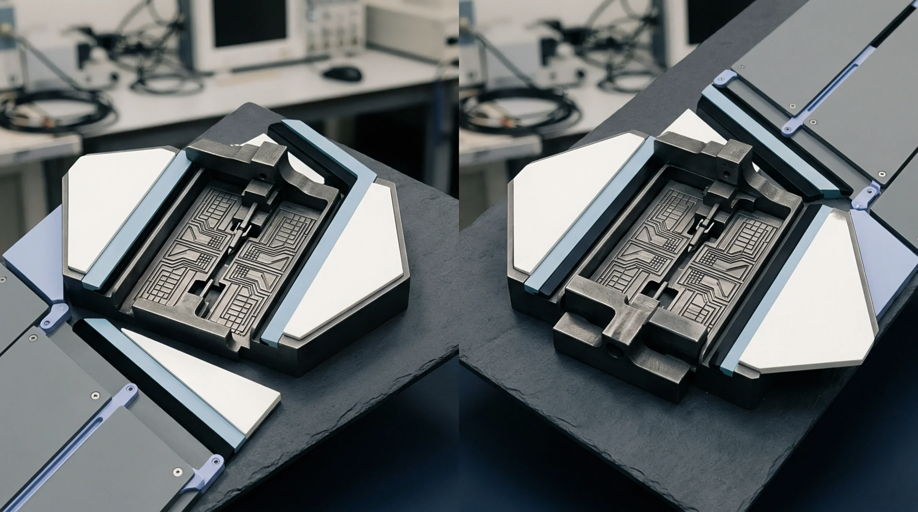
A planar transmission line architecture routes high frequency signals across a printed circuit board by placing a central conductor on the top dielectric layer flanked by two grounded return paths. High frequency signal integrity depends on this geometry because electric and magnetic fields distribute across the upper substrate surface without requiring a dedicated ground plane on the bottom layer. Radio frequency engineers calculate characteristic impedance from conductor width, slot gap dimensions and substrate relative permittivity.
Fabrication tolerances on trace width directly shift insertion loss metrics during final qualification testing.
Thermal Interface
Heat dissipation across microwave modules requires careful management of localized power density beneath active semiconductor devices. Thermal conductivity values for substrate materials dictate maximum operational current limits before carrier mobility degrades inside gallium arsenide amplifiers. Mechanical housing designers attach grounding blocks directly beneath the board footprint to transfer thermal energy away from the central conductor.
Manufacturing Tolerances
Etching precision during chemical processing determines phase matching across multichip radio frequency modules. Substrate thickness variations alter the effective dielectric constant and shift return loss signatures during vector network analyzer validation. Production facilities establish strict optical inspection gates to catch copper undercut defects before surface mount assembly.
Grounding Continuity
Parasitic mode suppression relies on frequent wire bond stitching between parallel ground planes on opposite sides of the dielectric stack. Electrical continuity failures at enclosure seams generate cavity resonances that corrupt transmission performance above ten gigahertz. Assembly technicians apply conductive epoxy along housing walls to eliminate ground loops prior to final sealing of the radio frequency compartment.