Statistical Tolerance Stackup Modeling for Millimeter Wave Printed Circuit Board Fabrication Handover Dossiers
Statistical tolerance dossiers must bridge mechanical etching distributions and high-frequency S-parameter gating to prevent mmWave panel scrap.


Foil
Copper cladding profiles dictate high-frequency insertion loss and phase stability above thirty gigahertz. At millimeter wave frequencies, the electrical skin depth decreases below six hundred nanometers, forcing the electromagnetic field to propagate almost entirely within the tooth structure of the metal-dielectric boundary. Standard electrodeposited foil exhibits a root-mean-square surface roughness exceeding one point five micrometers, which slows phase velocity and degrades transmission efficiency through local inductive retarding effects.
Fabricators working on automotive radar or E-band transceivers substitute very low profile or rolled annealed metal to bound these surface perturbations within three hundred nanometers.
Phase shifts compound rapidly.
Chemical etching introduces geometric distortion along the conductor sidewalls. Etch chemistry removes metal laterally while penetrating down to the dielectric base, converting an intended rectangular cross section into an inverted trapezoid. The difference between the top trace width and the bottom trace width defines the etch factor.
When processing fifteen-micrometer-thick copper foil, fabricators face etch undercut variations between five and twelve micrometers depending on spray nozzle calibration, etchant pool depth across inner panel zones, and conveyor velocity.
Treated copper surfaces with roughness values exceeding four hundred nanometers increase apparent microstrip line attenuation by more than twenty percent at seventy-seven gigahertz.
Narrow lines suffer severe undercutting.
Subtracting copper through standard panel-plating subtractive processing creates pronounced width distributions across large production panels. Semi-additive processing and modified semi-additive processing deposit copper into photoresist trenches, achieving vertical sidewall definitions with line-width tolerances held within two point five micrometers. These processing differences determine whether the characteristic impedance distribution remains inside acceptable radio frequency reflection boundaries.
- Rolled annealed copper features smooth grain boundaries that minimize high-frequency conduction losses on thin fluoropolymer cores.
- Electrodeposited reverse treated foil anchors microscopic zinc dendrites into the resin while presenting a flattened surface toward the signal trace body.
- Chemical micro-etch treatments modify copper surface topography before lamination, altering the interfacial roughness profile in ways standard profile gages fail to detect.
- Electroless nickel immersion gold introduces a ferromagnetic nickel barrier that adds unexpected attenuation on millimeter wave surface traces.
Failure to specify precise metal foil profiles and chemical treatment regimes in the fabrication dossier results in center frequency shifts on distributed planar filters, forcing costly scrap cycles during incoming quality inspection.

Variance
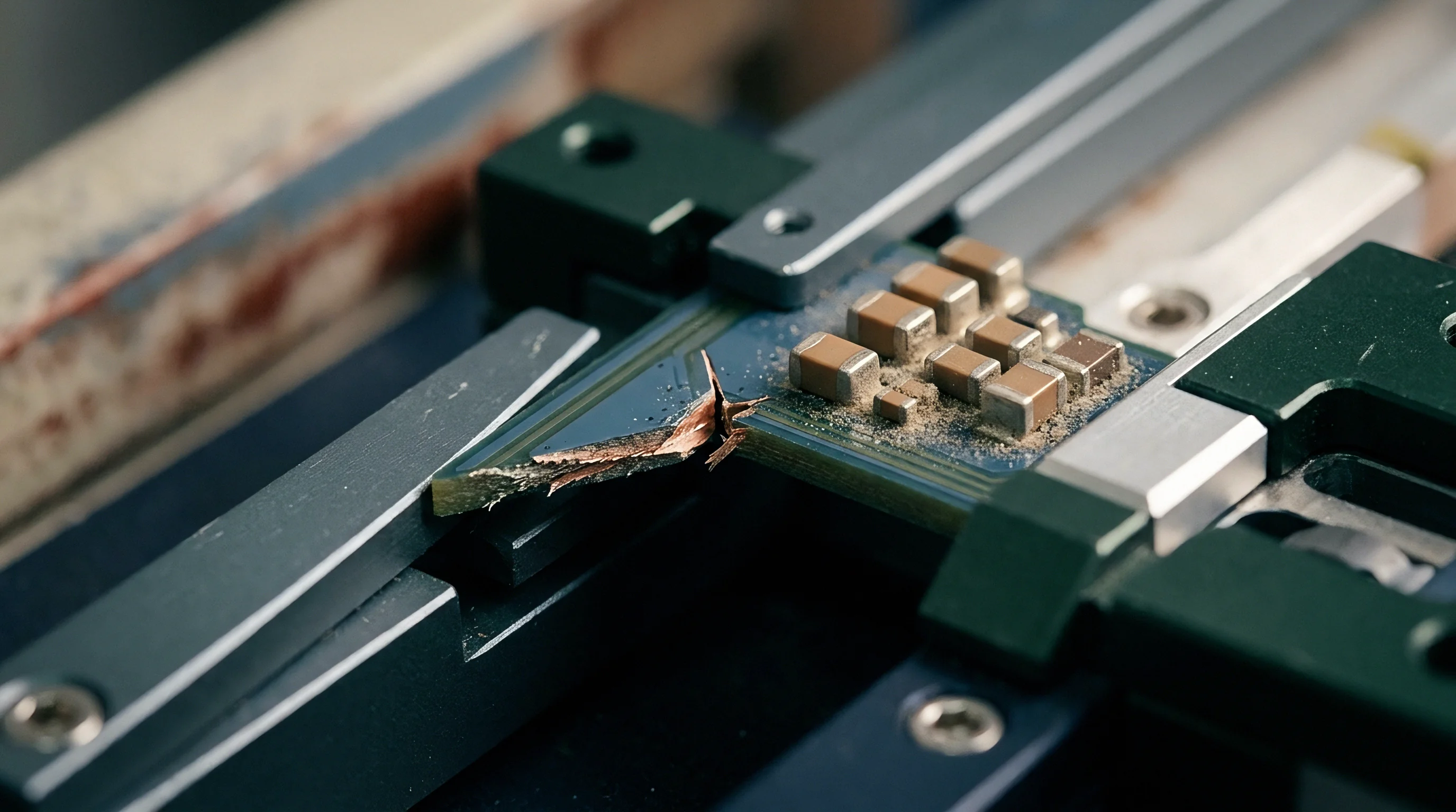
Dielectric substrates exhibit physical shifts across laminate production panels that disturb electromagnetic fields. High-frequency fluoropolymer, liquid crystal polymer, and reinforced hydrocarbon laminates specify nominal dielectric constants with tolerance envelopes between plus or minus zero point zero two and zero point zero five. These manufacturer specifications describe base resin blocks tested under clamped stripline conditions at ten gigahertz rather than microstrip transmission lines operating in the seventy-six to eighty-one gigahertz window.
Resin content alters propagation speed.
Lamination press cycles introduce localized height changes across multi-layer circuit boards. Glass-reinforced laminates utilize woven fabrics where fiberglass yarn bundles cross at defined mechanical pitches. The dielectric constant of woven E-glass sits near six point six, while hydrocarbon resin matrices range from two point one to three point zero.
When a transmission line runs parallel to the weave structure, the conductor alternately traverses glass knuckles and resin pockets, inducing a periodic impedance variation and localized phase skew.

Dielectric Constant Dispersion and Resin Inhomogeneity
Woven reinforcement styles directly dictate local permittivity distributions across the panel area. Style 106 glass delivers loose yarn placement with wide resin gaps, generating severe phase velocity fluctuations on millimeter wave conductors. Tighter styles such as 1078 or spread-glass 1035 spread the filament bundles flat, yielding a homogeneous dielectric substrate that damps localized phase deviations down to acceptable levels for phased-array radar feeds.
Substrate thickness variations compound these dispersion phenomena. Core thickness tolerances of plus or minus seven point five percent allow absolute dielectric height movements of seven to fifteen micrometers on thin millimeter wave cores. Because the fringing field capacitance depends inversely on the distance between the signal trace and the reference ground plane, vertical dimensional changes shift the transmission line characteristic impedance far more aggressively than horizontal etch variations.

Why Do Substrate Heights Dictate Phase Velocity?
Electromagnetic field energy distributes unevenly between the underlying dielectric medium and the air space surrounding an open microstrip line. Thinning the substrate concentrates a higher percentage of the field inside the dielectric bulk, elevating the effective dielectric constant and reducing phase velocity along the trace length. This physical mechanism translates small lamination pressure gradients directly into localized propagation delays.
Overetching shrinks line widths drastically.
Fabrication shops counter that raw material suppliers ship prepreg with intrinsic resin content variations of plus or minus two percent by weight, making localized thickness shifts inevitable whenever complex copper balance geometries draw unequal resin flow during press consolidation cycles.


Sensitivity
Derivatives relating electromagnetic phase constants to physical trace dimensions reveal distinct manufacturing dependencies. Designers often rely on simplified first-order Taylor series approximations to estimate how fabrication shifts alter circuit behavior. A Taylor series expansion treats each fabrication variable as an uncoupled parameter, calculating overall characteristic impedance variation through partial derivatives multiplied by individual parameter tolerances.
Simulation tools assume ideal edges.
Linear sensitivity analysis assumes the underlying physical processes operate in a symmetric, linear domain. At seventy-seven gigahertz, however, conductor cross-sectional changes interact nonlinearly with dielectric thickness movements. The fringing field capacitance between a trapezoidal conductor edge and an irregular copper ground plane does not scale proportionally with line width adjustments.
| Parameter | Nominal Value | Fabrication Tolerance | Partial Derivative (dZ0/dx) | Linear Delta Z0 |
|---|---|---|---|---|
| Trace Width (W) | 185.0 um | +/- 10.0 um | -0.22 Ohm/um | -/+ 2.20 Ohm |
| Dielectric Height (H) | 100.0 um | +/- 8.0 um | +0.41 Ohm/um | +/- 3.28 Ohm |
| Dielectric Constant (Dk) | 3.00 | +/- 0.04 | -8.15 Ohm/unit | -/+ 0.33 Ohm |
| Copper Thickness (T) | 18.0 um | +/- 3.0 um | -0.08 Ohm/um | -/+ 0.24 Ohm |
| Etch Factor (Base/Top) | 1.25 | +/- 0.15 | -1.80 Ohm/unit | -/+ 0.27 Ohm |
Calculated nominals rarely survive production.

Linear Root Sum of Squares Limitations
Root sum of squares techniques aggregate tolerance limits under the assumption that all manufacturing errors follow normal Gaussian probability density functions centered perfectly at the nominal design point. In printed circuit board fabrication, chemical etch processes exhibit pronounced skewness: bath depletion, conveyor shadowing, and copper density gradients systematically bias the distribution toward lower trace widths. Summing asymmetric parameters through conventional root sum of squares methods underestimates total impedance drift by failing to capture the physical skew of chemical etching.
Dielectric dispersion destroys filter bandwidth.
The IPC-6012DA specification restricts high-frequency automotive radar microstrip impedance excursions to within plus or minus five percent of nominal design values on qualified coupon structures.
Worst-case analysis calculates the direct sum of parameter extrema, yielding extreme impedance boundaries that force circuit designers to demand unattainable production tolerances. Applying worst-case bounds to high-frequency patch arrays leads buyers to reject panels that would otherwise operate within full system link-budget requirements.

Nonlinear Monte Carlo Yield Boundaries
Numerical Monte Carlo simulation solves nonlinear tolerance compounding by sampling multi-dimensional parameter distributions simultaneously. By assigning empirical probability distributions to dielectric thickness, conductor top width, conductor bottom width, and surface roughness parameters, the numerical engine captures physical coupling between variables. A thinned dielectric combined with an over-etched trace creates localized field concentrations that linear models miss entirely.
Tooling files govern final geometry.
A Monte Carlo run executing twenty thousand iterations provides realistic yield projections for distributed structures such as branchline couplers, stepped-impedance filters, and quarter-wave matching transformers. By tracking return loss and insertion loss distributions directly against electrical circuit goals, the engineer identifies which fabrication tolerance dominates circuit failure without over-specifying adjacent non-critical dimensions.
Substrate thickness variations override conductor etching tolerances whenever the dielectric height falls below one hundred micrometers.


Coupon
Test fixtures integrated into panel breakaways provide empirical verification of high-frequency propagation characteristics. Standard mechanical cross sections expose physical trace geometry, copper plating thickness, and dielectric thickness under optical or scanning electron microscopes. Destructive physical cross sections, however, provide zero direct data regarding the high-frequency permittivity, loss tangent, and surface roughness interactions governing circuit function.
Microstrip losses double past fifty gigahertz.
High-frequency characterization relies on dedicated radio frequency coupons measured with calibrated vector network analyzers. Automated wafer probers apply ground-signal-ground microprobes directly to coupon launch structures on the production panel edge. Thru-Reflect-Line calibration standards embedded within the panel frame de-embed test fixture and probe transition parasitics, delivering unambiguous extraction of complex propagation constants up to one hundred and ten gigahertz.
| Coupon Structure | Target Parameter | Measurement Method | De-Embedding Technique | IPC Reference |
|---|---|---|---|---|
| Differential Phase Line | Effective Dk / Dispersion | VNA Transmission Phase | TRL or multiline TRL | IPC-TM-650 2.5.5.5 |
| Ring Resonator | Bulk Dielectric Constant | VNA S21 Resonant Peak | Loose Coupling Gaps | IPC-TM-650 2.5.5.6 |
| Single-Ended Microstrip | Characteristic Impedance | TDR / S11 Time Domain | Gating / 2x-Thru | IPC-TM-650 2.5.5.7 |
| Cross-Section Coupon | Etch Factor / Trace Width | Optical Microsection | Visual Graticule / SEM | IPC-TM-650 2.1.1 |
Tight margins elevate substrate pricing.

Test Vehicle Topologies for in Situ Extraction
Transmission line coupons must mirror the exact electromagnetic stackup of the active radio frequency board area. Placing ground coplanar waveguide test coupons in panel locations with low copper density induces copper plating thickness variations that do not reflect the dense trace environment of an antenna feed network. The physical placement of coupons requires careful balancing against internal plane patterns to preserve representative plating current densities.
- Thru-Reflect-Line calibration coupons must reside within five centimeters of active board edges to capture representative lamination thickness values across the panel area.
- Differential line length pairs require length deltas exceeding two guided wavelengths at the lowest test frequency to prevent measurement noise from corrupting calculated phase velocity values.
- Ring resonator geometries isolate bulk substrate permittivity from conductor etching errors by extracting resonant frequencies determined primarily by geometric circumference rather than trace width.
- High-speed microsection patterns position sacrificial target pads along both conveyor axes, revealing spatial etching discrepancies between leading and trailing panel edges.

Should Millimeter Wave Handover Enforce S Parameter Gating?
Fabrication contracts frequently restrict acceptance criteria to direct-current resistance or low-frequency time-domain reflectometry impedance coupons measured at one gigahertz. A board passing time-domain impedance testing at two gigahertz can fail completely at seventy-seven gigahertz due to untracked surface roughness degradation or weave skew. Handover documentation must stipulate high-frequency S-parameter mask verification directly on panel breakaways.
Scrap rates climb without calibration.
A production lot rejected under IPC-6012DA Clause 3.6.2.1 for high-frequency transmission loss non-conformance releases the purchasing organization from inventory acceptance obligations regardless of direct-current continuity test results.


Yield
Statistical process capability indices determine whether a production line satisfies radio frequency distribution windows. Module developers routinely stipulate a capability target of one point three three for critical dimensions, which demands that the total process spread occupies no more than seventy-five percent of the allowable specification range. Standard process capability calculations assume stable Gaussian output centered symmetrically within upper and lower specification limits.
Etch chemistry creates systematic drift.
Real-world printed circuit board manufacturing facilities exhibit continuous process drift driven by chemical bath loading, temperature variations across lamination platens, and mechanical drill wear. To capture process centering offsets alongside broad variance distributions, the handover dossier demands tracking the process capability index Cpk, which accounts for the distance between the process distribution mean and the nearest specification boundary.

Process Capability Metrics under Skewed Distributions
When parameter distributions exhibit significant skewness or bimodal peaks, standard Cpk equations inflate reported process capability. In microstrip transmission lines, over-etching creates a long tail toward narrow line widths, while mechanical lamination pressure gradients skew thickness toward the lower boundary. Evaluating these features requires Box-Cox transformations or Johnson family curve-fitting to normalize empirical data before computing final capability metrics.
The fabricator shifts blame downward.
Contractual boundaries depend on whether capability metrics apply to physical dimensions or to functional electromagnetic properties. A fabricator capable of delivering a Cpk of one point five on physical trace width can still generate an electrical impedance Cpk below one point zero if the raw substrate supplier delivers dielectric cores exhibiting unmonitored permittivity drift.

Worked Extraction on Radar Front End Feeds
Consider an automotive radar microstrip patch feed network designed for seventy-seven gigahertz on a nominal one-hundred-micrometer core with a nominal dielectric constant of three point zero zero. The electrical requirement mandates a characteristic impedance of fifty ohms with an allowable system tolerance of plus or minus two ohms, establishing an upper specification limit of fifty-two ohms and a lower specification limit of forty-eight ohms. The physical trace width targets one hundred eighty-five micrometers.
Assume the fabricator runs a pre-production trial of one hundred panels, collecting high-frequency coupon extractions across the run. Physical microsections indicate a mean trace width of one hundred eighty-three micrometers with a standard deviation of two point five micrometers. Dielectric height measurements reveal a mean of ninety-eight micrometers with a standard deviation of two point zero micrometers.
Dielectric constant measurements show a mean of three point zero one with a standard deviation of zero point zero one five.
Propagating these empirical distributions through the electromagnetic transmission line equations yields a calculated impedance distribution. The mean characteristic impedance arrives at fifty point six ohms. The resulting standard deviation of the characteristic impedance equals zero point eight five ohms.
Calculating the process capability indices under these extraction results:
The upper capability index equals fifty-two minus fifty point six divided by three times zero point eight five, yielding zero point five five. The lower capability index equals fifty point six minus forty-eight divided by three times zero point eight five, yielding one point zero two. The overall process capability index Cpk sits at zero point five five, falling far below the target value of one point three three.
Although every physical manufacturing parameter remained within catalog tolerances, the combined statistical distribution produces an electrical scrap rate exceeding five percent. This worked example demonstrates that managing physical dimensional tolerances independently fails to assure millimeter wave electrical compliance.
Will fabricators accept functional S-parameter yield loss liabilities when raw material suppliers decline to guarantee batch-level permittivity distributions above forty gigahertz?

Custody
Design handover packages establish technical and commercial boundaries between module developers and manufacturing facilities. When transitioning a millimeter wave design from prototype validation to volume manufacturing, ambiguous documentation creates unassigned commercial risk. A standard fabrication drawing containing general IPC Class 3 notes lacks the explicit statistical definitions required to control high-frequency phase and impedance distributions.
Contractual boundaries settle scrap disputes.
The engineering handover dossier must contain comprehensive digital datasets, rigorous stackup definitions, statistical process capability targets, and concrete coupon measurement procedures. Modern digital fabrication formats supersede legacy files by embedding physical material assignments and tolerance limits directly into production tooling.
Handover Package Schema and Artifact Formats
A rigorous millimeter wave fabrication release replaces traditional Gerber RS-274X data with IPC-2581C or ODB++ design databases. These intelligent formats integrate schematic netlists, layer-specific material properties, controlled impedance line identifiers, and coupon geometries into a single verified archive. The transfer file eliminates manual data entry by the board fabricator, preventing geometry translation errors during computer-aided manufacturing engineering review.
- Intelligent design exchange files formatted in IPC-2581C designate millimeter wave nets, line-width compensation rules, and target layer registrations without ambiguous external drawing text.
- Controlled stackup documentation specifies supplier-specific core and prepreg part numbers, glass weave styles, nominal resin contents, and cured dielectric thicknesses.
- Panel coupon placement maps dictate the exact spatial positions of high-frequency test coupons on breakaway rails relative to internal copper balance zones.
- Touchstone S-parameter acceptance templates define vector network analyzer frequency grids, port calibration requirements, and pass-fail mask limits for production panel signoff.
- Microsection measurement protocols establish target inspection planes for trapezoidal trace width, plating thickness, and dielectric thickness verification under calibrated optical microscopes.
Division of Financial Liability for out of Band Shifts
Commercial contracts governing millimeter wave board fabrication must delineate responsibility between design flaws and manufacturing non-conformance. When a manufactured batch displays resonant filter shifts that exceed system tolerances, disputes arise regarding root cause attribution. If the fabricator built all traces, spaces, and substrate thicknesses within agreed mechanical tolerances, the financial burden of scrap rests with the design organization.
To protect capital investment, the handover agreement must link final lot acceptance to explicit coupon performance metrics rather than bare dimensional compliance. The contract stipulates that the fabricator owns process drift, chemical variations, and etching skew up to the delivery of conforming high-frequency test coupons. The buyer assumes commercial responsibility for nominal design choices once coupon S-parameters fall within the modeled statistical window established in the handover dossier.
Clear documentation protocols transform subjective factory disputes into deterministic engineering verifications, protecting both parties during volume production scaling.