Resolving Multi National Process Patent Conflicts in Cross Border Heterogeneous Packaging Transfer Dossiers
Reconciling cross-border packaging dossiers requires mapping recipe parameters against territorial process patents and enforcing parameter limits in SOW contracts.
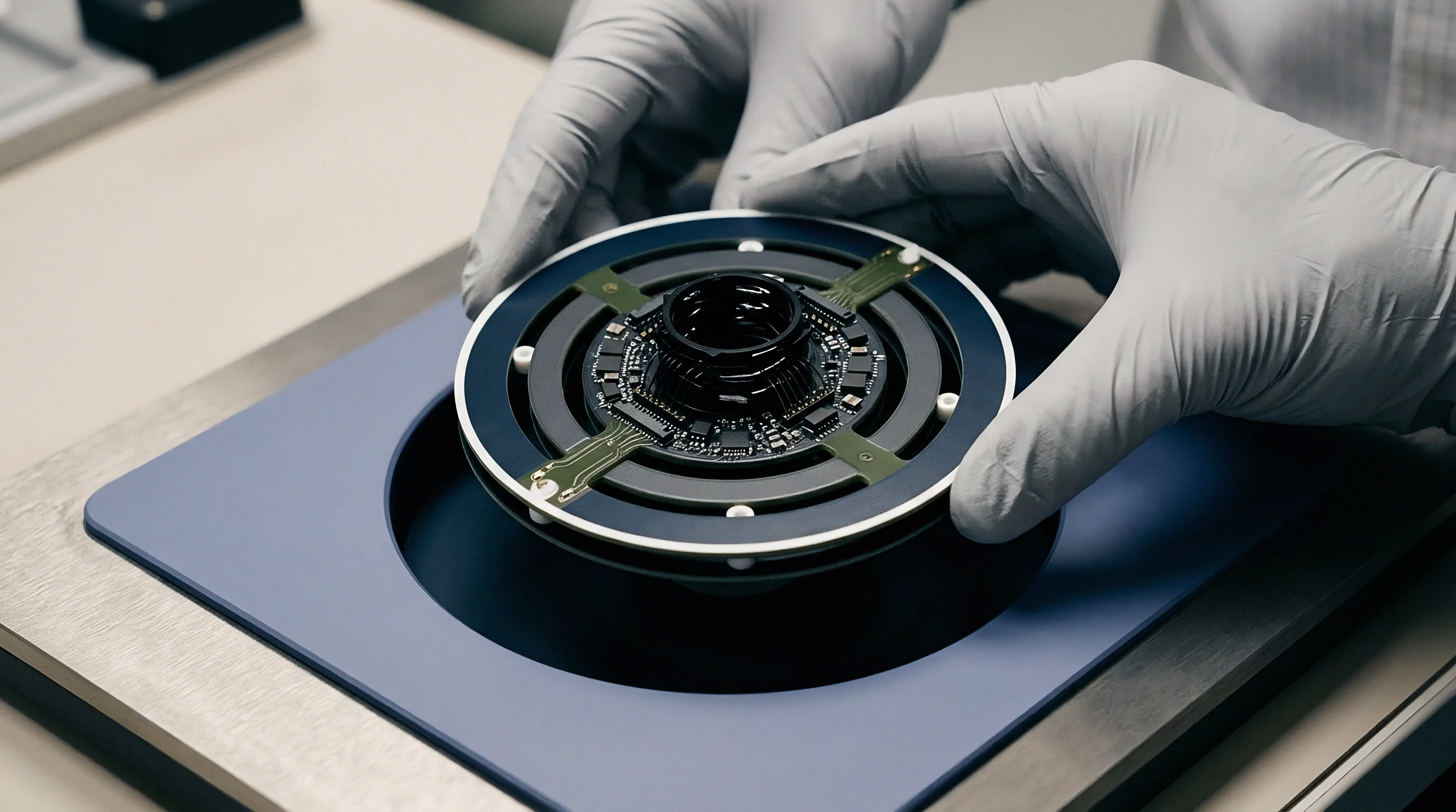

Wafer
Heterogeneous Packaging Mechanisms and Territorial Claim Exposure
Cross-border semiconductor manufacturing increasingly relies on multi-chiplet integration where distinct functional dies assemble onto a single silicon interposer or organic substrate. Modern high-density interconnect structures employ fine-pitch copper-to-copper direct bonding, high-aspect-ratio through-silicon vias, and microbump arrays operating below twenty micrometers pitch. When assembly design kits and manufacturing recipe sets cross international boundaries, the physical processes performed on the silicon die face distinct regional patent monopolies.
Thermal compression bonding sequences optimized for minimal warpage in one jurisdiction frequently fall directly within process patent claims granted under a neighboring patent office. A physical packaging process executable in Taiwan without license exposure can trigger immediate utility patent infringement actions upon reaching a semiconductor foundry in South Korea or a packaging facility in Germany.
Process patent claims in advanced microelectronics packaging focus on physical operational parameters rather than final physical topology alone. Patent offices examine specific thermodynamic sequences, chemical-mechanical planarization surface roughness targets, plasma activation surface energy thresholds, and temperature ramp rates during intermetallic compound growth. A transferred packaging dossier contains exact numerical parameters for vacuum chamber pressures, argon ion bombardment power levels, and furnace annealing duration.
If a transfer package instructs a target OSAT line to perform dielectric activation at two hundred fifty degrees Celsius under a specified oxygen plasma flow rate, that instruction directly instigates the patented method within the destination country. Yield drops without planarization.
Thermal compression bonding profiles executed at two hundred eighty degrees Celsius under five megapascals pressure trigger method claim matches across four distinct European patent families when pad pitch drops below fifteen micrometers.
Differences in national patent laws compound process conflict risk across cross-border assembly operations. United States patent enforcement extends to imported physical goods manufactured abroad through process steps patented under domestic law. A package assembled in Southeast Asia using a process patented in the United States faces customs seizure or exclusion orders upon import, even if the manufacturing location grants no process patent protection for that method.
Conversely, European jurisdictions evaluate process patent infringement strictly based on local execution of method steps, creating asymmetric legal exposure between the foundry country and the destination market. Process files carry liability.
Physical Parameter Sensitivity and Infringement Mapping
Evaluating heterogeneous assembly transfer packages requires matching mechanical and chemical recipe parameters against independent method claims across target manufacturing jurisdictions. Die attach operations, surface activation steps, and mold underfill dispensing methods exhibit narrow physical operating windows. Adjusting process temperatures or chemical compositions to bypass patent claims often alters intermetallic compound formation, leading to voiding, delamination, or early thermo-mechanical fatigue.
The transition from solder microbumps to direct copper-to-copper hybrid bonding illustrates this physical boundary. Direct hybrid bonding relies on ultra-clean planar surfaces where dielectric layers and metallic contacts bond at room temperature before undergoing thermal annealing. Patents governing this domain claim precise surface topography metrics, such as root-mean-square surface roughness under zero point three nanometers, alongside specific plasma activation chemistries.
A packaging dossier specifying an nitrogen-hydrogen plasma treatment for ten seconds at one hundred watts power may land squarely inside an active process patent held by a competitive OSAT in the target country.
Substrate thickness limits warpage. Modifying plasma activation durations or substituting silane chemistry shifts bonding energy, forcing furnace annealing temperatures to increase from two hundred degrees to three hundred fifty degrees Celsius. Thermal profiles dictate infringement.
Higher thermal budgets introduce unacceptably high mechanical strain across large chiplet assemblies, causing silicon die warping and fine-pitch interconnect fractures. Engineering teams must map every physical threshold within the assembly recipe against active territorial patent claims before releasing manufacturing dossiers to cross-border production facilities.
Failure to reconcile regional method claims before committing tooling and assembly line capacity results in total shipment halts at destination ports, broad preliminary injunctions that lock production equipment, and cumulative NRE write-offs exceeding three million dollars per chiplet product line.
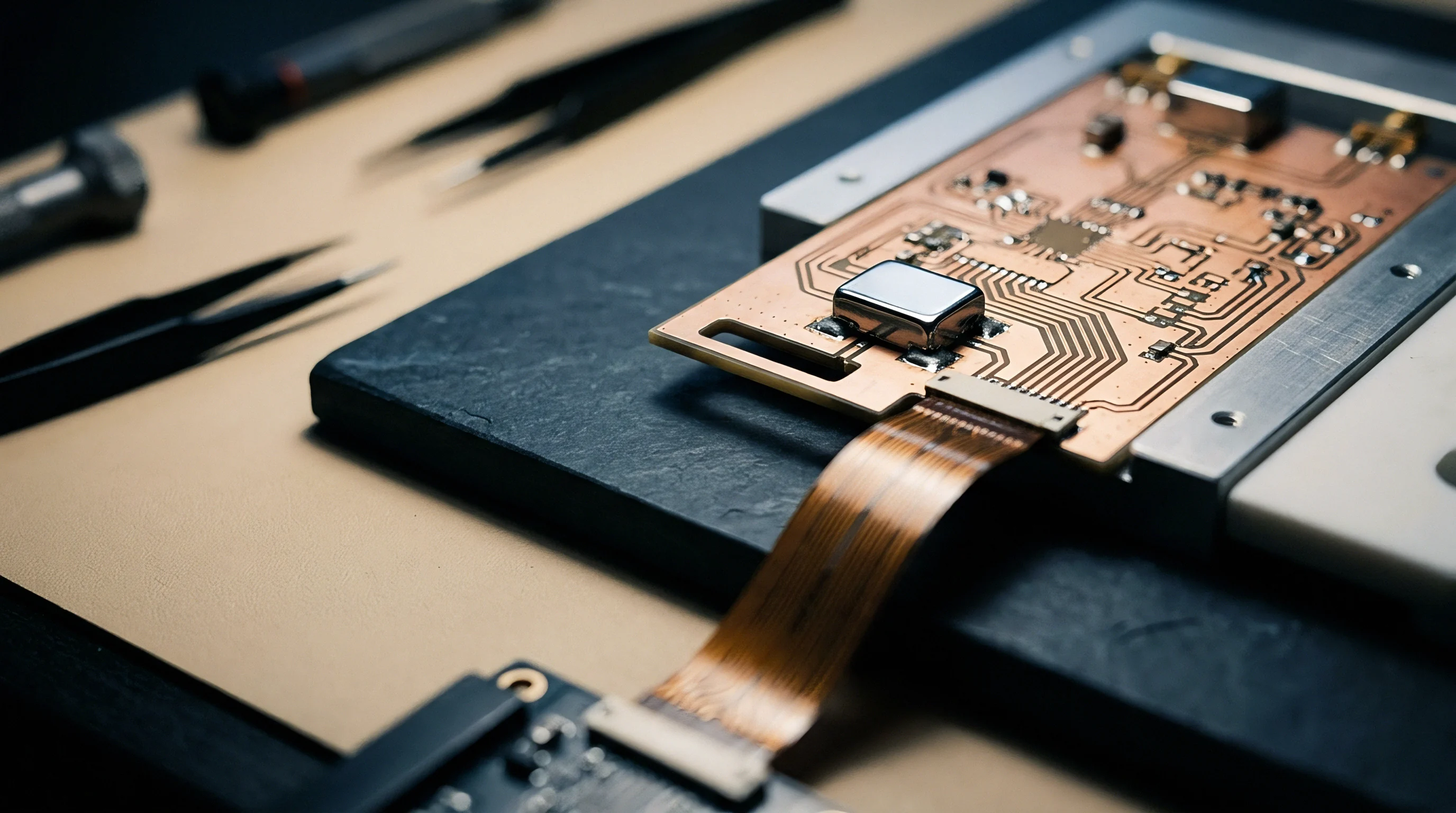

Mapping
Packaging Transfer Dossier Structural Analysis
Assembly design transfer packages convert electronic design automation outputs into physical manufacturing commands. A complete transfer dossier for heterogeneous packaging contains layout data, process design kits, assembly design kits, bill of materials documentation, and factory equipment program files. Layout information arrives in Graphic Data System II or Open Access System Interchange Standard files specifying redistribution layer geometries, pad placement, and passivating openings.
Fabrication parameters reside inside text-based recipe formats governing wafer dicing, pick-and-place placement accuracy, mold compound curing cycles, and laser drilling profiles.
Process patent conflicts manifest when raw recipe files contain instructions that mirror method claims registered in the target manufacturing territory. High-density redistributed layer processes rely on multi-step chemical etch and electroplating sequences to form sub-micron line and space widths. Standard design transfers pass these process steps as fixed recipe parameters to guarantee impedance matching and current density performance.
The destination facility receives executable code for automated plating lines that directly implements patented current density modulation or additive bath chemistries. Jurisdictions evaluate file transmission and machine programming as acts of inducement or direct infringement depending on local statutory definitions.
Packaging dossiers split into discrete technical files, each carrying explicit process parameters vulnerable to territorial patent claims. The following set identifies core components within a transfer package that expose assembly programs to regional legal challenges:
- Redistribution Layer Electroplating Parameters specify exact chemical bath additives, pulse current densities, and agitation rates that form fine-pitch copper traces without voiding.
- Direct Hybrid Bonding Recipes dictate plasma chamber atmosphere, radio-frequency power, exposure duration, and chemical-mechanical polishing slurries required for copper-dielectric planarity.
- Laser Via Drilling Sequences define pulse frequency, energy density per pulse, and beam shaping profiles used to form sub-thirty micrometer micro-vias through interposer dielectrics.
- Underfill Capillary Flow Instructions describe substrate pre-heating profiles, dispensing needle motion paths, fluid viscosity limits, and two-stage furnace cure schedules.
- Wafer Thinning and Backside Metallization Schedules list grind wheel grit sizes, chemical-mechanical planarization removal rates, stress-relief etch times, and sputter deposition power levels for back-side power distribution grids.

Cross-Territorial Dossier Conflict Analysis
Resolving territorial process conflicts demands systematic cross-referencing between packaging dossier parameters and patent office databases across manufacturing locations. An assembly step execution that is completely unencumbered under Taiwanese patent records can trigger litigation under United States or European patent grants. Engineering teams compare process window limits against independent method claim boundaries to locate operational intersections.
The structured comparison below correlates heterogeneous packaging transfer deliverables with their specific physical process parameters, target patent claim types, and cross-border commercial exposure levels:
| Dossier Deliverable | Embedded Physical Recipe | Target Patent Claim Type | Cross-Border Risk Exposure |
|---|---|---|---|
| GDSII / OASIS RDL Layout | Sub-micron trace spacing and passivating aperture dimensions | Physical structure and layout topography claims | High import exclusion risk at border control points |
| Hybrid Bonding Recipe Set | Plasma activation power, pressure, gas mixture, anneal thermal curve | Method of surface activation and low-temperature diffusion bonding | Direct line injunction risk at destination OSAT facility |
| TCB Machine Tooling File | Bond head force profile, laser ramp rate, temporary adhesive release | Method of thermal compression bonding under variable load | Inducement of infringement claims against design house |
| CMP Slurry & Pad Schedule | Abrasive particle size distribution, pad down-force, slurry pH value | Chemical-mechanical planarization process for co-planar Cu/oxide | Supplier liability and indirect patent infringement disputes |
| Capillary Underfill Program | Dispense trajectory, substrate temperature, edge bead cure profile | Method of void-free underfill encapsulation in multi-chiplet stack | Process patent enforcement upon finished package teardown |
File formats record ownership. When requested to modify recipe steps that breach local process patents, contract packaging facilities consistently state that altering factory-qualified process files destroys yield warranties and transfers full financial responsibility for assembly defects back to the design house.

Recipe

Engineering Protocols for Process Design-Around
Bypassing conflicting process patent claims without compromising microelectronic package reliability requires systematically modifying assembly steps. Process engineers must adjust manufacturing parameters outside the literal scope of valid patent claims while maintaining operation inside the functional assembly yield window. This practice demands precise characterization of material behavior, thermal expansion matching, and mechanical strain mitigation.
When an active patent claims a surface activation method using pure oxygen plasma at fifty watts power for twenty seconds, process designers evaluate alternative chemical species and energy profiles. Interposer pitch defines density. Substituting an argon-nitrogen gas mixture at eighty watts power for eight seconds alters ion bombardment kinetics and surface radical density.
The modified sequence must produce equivalent surface energy, exceeding sixty-five millijoules per square meter, to achieve void-free copper-to-copper bonding during subsequent room-temperature contact. Plasma activation alters bonding.
Altering chemical-mechanical polishing slurry abrasive concentration by five weight percent alters oxide removal rates, requiring real-time optical endpoint monitoring to prevent copper recess variations beyond four nanometers.
The systematic protocol for executing an engineering design-around within a cross-border packaging dossier follows a strict procedural sequence:
- Extract all numerical constraints from independent claims of active process patents in target manufacturing territories.
- Perform physical response surface methodology testing to establish functional operating boundaries for temperature, pressure, time, and chemical exposure.
- Select alternative process parameters that clear patent claim limits by a minimum twenty percent safety margin while remaining within established assembly yield limits.
- Re-validate mechanical interconnect integrity through temperature cycling testing from minus fifty-five to one hundred twenty-five degrees Celsius across one thousand thermal cycles.
- Update machine configuration files, assembly design kit parameters, and quality inspection criteria across the entire packaging design transfer package.
- File defensive technical disclosures or updated patent applications covering the modified process parameter combination.

Whose Liability Governs Process Patent Infringement in Multi-Foundry Packaging Flows?
Multi-foundry supply chains split manufacturing responsibilities across multiple independent entities. A silicon interposer originates at a wafer foundry in one country, receives redistributed layers at an independent interposer house, undergoes die attach at an OSAT in a second country, and completes final mold encapsulation at a third facility. Identifying which party bears legal liability for process patent infringement depends on where each physical method step executes and how the statement of work structures technical instructions.
If a design house provides explicit, unalterable machine control scripts that instruct an OSAT to perform a patented process, courts frequently identify the design house as the primary party inducing infringement. Conversely, if the design house provides only performance specifications, leaving the OSAT to select specific process recipes, liability shifts toward the manufacturing facility. Tooling changes require approval.
Solder reflow shifts stress.
Modifying process parameter boundaries beyond twenty percent of original equipment vendor defaults destroys baseline assembly yield unless furnace profiles, placement forces, and chemical bath agitation rates undergo simultaneous re-optimization.


Cleavage

Split-Foundry Integration and Intermediate Assembly Boundaries
Managing heterogeneous packaging transfers across conflicting patent jurisdictions often requires splitting assembly processes between geographic locations. Split-foundry manufacturing separates sensitive process steps, assigning high-risk operations to regions where patent grants have expired, where freedom-to-operate licenses exist, or where local patent claims do not cover the specific process variant. An intermediate wafer substrate undergoes initial processing in one country, travels across borders under strict export classification codes, and completes assembly at a secondary location.
A primary challenge in split-foundry arrangements involves defining clean physical handover boundaries between facilities. Intermediate packaging structures, such as diced interposer wafers mounted on tape frames or partially stacked chiplet assemblies, exhibit extreme sensitivity to surface oxidation and organic contamination. Wafer storage duration between split process steps directly affects contact resistance and bond strength.
Transporting exposed copper microbumps across maritime boundaries requires vacuum-sealed carrier packaging under controlled inert gas backfill to prevent native oxide growth exceeding two nanometers thickness.
Cleanroom audits reveal line parameters. Cross-border handovers of intermediate silicon structures require precise physical specifications at each cleavage plane. Engineering teams deploy formal evaluation criteria to assess whether a packaging workflow should split across geographic lines:
- Surface Passivation Stability measures the rate of native oxide growth and ambient contamination pickup on exposed metallic pads during international transit.
- Test Coupon Accessibility provides dedicated probe pad areas on intermediate interposers to verify electrical continuity and trace impedance before shipping to secondary OSAT facilities.
- Thermal History Accumulation tracks total thermal exposure hours across sequential assembly steps to prevent premature aging or grain growth in intermetallic interconnects.
- Export Compliance Classification determines whether intermediate packaging transfer files, lithography masks, or modified process recipes trigger dual-use technology export restrictions.
- Dossier Partitioning Integrity enforces strict isolation between territorial recipe files, preventing target facilities from accessing process instructions non-essential to their specific assembly steps.

Intermediate Testing and Boundary Verification
Splitting process steps across cross-border OSAT facilities creates complex liability disputes when final package yields drop. Without rigorous intermediate testing at the cleavage boundary, identifying whether defects stem from primary wafer processing or secondary assembly steps becomes impossible. Intermediate testing protocols employ dedicated silicon test coupons integrated into scribe lines or scrap tile areas on the interposer wafer.
Standardized test structures measure chain resistance across through-silicon vias, dielectric isolation leakage currents, and redistribution layer line resistance. According to IEEE 1500 boundary-scan standards for embedded core test, intermediate die-to-die interconnects require built-in self-test hardware to verify signal integrity before encapsulation. Passing electrical verification at the cleavage plane establishes a clear legal and operational boundary, transferring custody and quality liability from the primary interposer vendor to the secondary packaging house.
Unregistered code risks injunction. Inspection coupons reveal steps.
Under SEMI E187 specifications for semiconductor equipment cybersecurity, transferred process files must carry cryptographic signatures to prevent unauthorized recipe modifications at destination facilities.
The unresolved operational challenge in cross-border split packaging remains whether cryptographic process locking on factory equipment can legally shield design houses from indirect patent infringement claims when local machine operators bypass software limits to recover line yield.

Stipulation
Commercial Contracts and Freedom-to-Operate Warranties
Commercial agreements governing cross-border packaging transfers must translate complex process patent allocations into clear financial and legal obligations. Master services agreements and statements of work define whether a project executes as a turnkey scope, a semi-custom development, or a reference design transfer. Each integration level carries distinct risk profiles regarding non-recurring engineering charges, process patent indemnification, and freedom-to-operate guarantees.
Turnkey packaging contracts place full responsibility for process selection, yield guarantees, and intellectual property clearance on the packaging supplier. The supplier warrants that its internal process recipes and equipment sequences infringe no third-party method claims within agreed manufacturing and distribution territories. Conversely, white-label and semi-custom transfer agreements shift process patent risks back to the design house.
In semi-custom arrangements, the customer supplies explicit layout files, bill of materials constraints, and target manufacturing process flows, leaving the supplier liable only for uninstructed equipment adjustments.
The table below details financial liabilities, freedom-to-operate warranty levels, and NRE cost structures across primary engineering integration models:
| Integration Level | Process Control Ownership | FTO Warranty Scope | NRE Pricing Range (USD) | Process Indemnification Allocation |
|---|---|---|---|---|
| Turnkey Packaging SOW | OSAT retains complete recipe ownership | Full worldwide freedom-to-operate warranty | $450,000 – $1,200,000 | Supplier holds total financial liability capped at contract value |
| Semi-Custom Transfer | Shared control; Customer specifies flow, OSAT adapts line | Territorial warranty limited to core OSAT processes | $250,000 – $750,000 | Liability split based on recipe parameter origin |
| Reference Design ADK | Customer owns full dossier and machine parameters | No process FTO warranty provided by foundry | $100,000 – $350,000 | Customer bears absolute liability for method infringement |
| White-Label Assembly | OSAT standard qualified packaging baseline | Standard OSAT process indemnity clause | $50,000 – $150,000 | Indemnification limited to direct baseline process claims |
Contractual Risk Mitigation Mechanisms
Constructing resilient cross-border packaging transfer contracts requires incorporating explicit freedom-to-operate verification milestones directly into payment schedules. NRE milestones must depend not only on physical package delivery and thermal reliability passing, but also on verified territorial process patent clearing. Data files carry legal consequences.
Transfer agreements require dedicated documentation standards to defend against cross-border process patent disputes. A complete legal and technical transfer pack includes the following contractually mandated deliverables:
- Territorial Freedom-to-Operate Assessment Reports provide certified legal and technical patent searches covering all target manufacturing and destination commercial markets.
- Process Parameter Source Matrices document the exact origin, engineering justification, and ownership of every parameter within assembly design transfer packages.
- Non-Infringement Engineering Certificates carry formal approval signatures from licensed process engineers attesting that modified parameter windows clear registered method claims.
- Third-Party License Sublicensing Agreements supply explicit legal authorization documents for any patented process steps incorporated directly into the assembly flow.
- Subcontractor IP Pass-Through Covenants ensure secondary OSAT facilities, substrate suppliers, and testing houses observe identical patent indemnification and confidentiality boundaries.
To establish clear contractual boundaries, legal counsel inserts dedicated process patent allocation clauses directly into packaging transfer agreements:
Section 8.4 of the Model Heterogeneous Packaging Transfer Agreement specifies that the customer retains sole financial responsibility for method patent infringement claims arising directly from mandatory recipe instructions provided in writing by the customer, whereas the supplier indemnifies the customer against all third-party process patent actions stemming from supplier-selected equipment parameters, slurry chemistries, or baseline factory assembly flows.

Dossier

Bring-Up Verification and Physical Reverse Engineering Defense
Final acceptance of a cross-border packaging transfer dossier depends on physical verification performed during initial bring-up builds. Engineering teams receive prototype lots from target OSAT facilities to verify that line parameter adjustments successfully cleared territorial patent claims without introducing subtle physical defects. Physical bring-up checks require destructive physical analysis, cross-sectional scanning electron microscopy, and energy-dispersive X-ray spectroscopy to confirm that physical package characteristics match modified recipe files.
Competitors and patent holders frequently execute reverse engineering teardowns on commercial packaging to identify potential process patent violations. Scanning electron micrographs reveal dielectric layer thicknesses, grain boundaries in copper interconnects, intermetallic compound compositions, and chemical-mechanical polishing dishing effects. If an OSAT fails to maintain strict control over modified slurry down-force parameters, physical copper erosion patterns on finished interposers can serve as direct circumstantial evidence of patented polishing methods in enforcement litigation.
Cross-sectional electron microscopy revealing an intermetallic compound thickness under one hundred nanometers at the copper-tin interface provides physical evidence of low-temperature diffusion bonding profiles executed below two hundred degrees Celsius.
Maintaining a clean legal position across multi-national packaging programs requires exhaustive configuration control over design transfer dossiers. Every revision of layout GDSII data, packaging design kits, bill of materials lists, and automated recipe scripts must carry full audit trails detailing legal clearance status across all manufacturing jurisdictions. When engineering teams modify a single thermal compression bonding parameter to clear a newly granted European patent, that change must automatically propagate across all derivative manufacturing dossiers, assembly design kits, and factory quality assurance files worldwide.
Verification protocols extend beyond physical hardware to encompass the software repositories and build environments that generate automated packaging recipes. Standardized digital signing of process files using cryptographic key pairs prevents unauthorized parameter alterations by local line operators attempting to boost assembly yield. Production equipment in destination OSAT facilities reads signed machine control files, executing only validated process windows that maintain legal non-infringement status.
Systematic alignment between physical parameter boundaries, territorial patent analysis, cryptographic file verification, and clear contractual indemnification lines creates a defensible, resilient cross-border manufacturing model for advanced heterogeneous packaging transfer programs.