Meaning
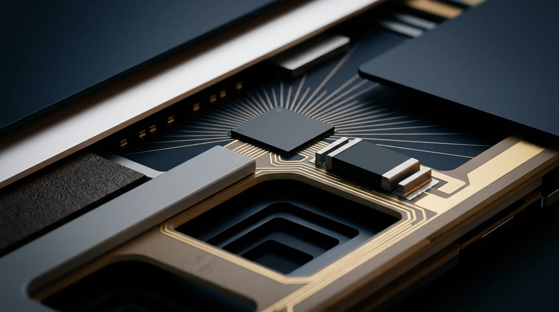
Advanced semiconductor packaging requires routing signals from the dense pad layout of a silicon die to the wider spacing of a printed circuit board. The redistribution layer is an additional layer of metal and dielectric deposited on the surface of the wafer to route the on-chip pads to alternative locations. This layer enables the use of larger, more robust solder balls for the board connection.
It is a prime component of wafer-level packaging.
Interconnect Routing
Standard silicon pad pitches are often too fine for direct surface mounting on a standard board. The redistribution layer acts as an adapter, routing the tightly packed signals outwards to a wider array of contact points. This routing helps simplify the design of the main board by reducing the need for expensive high-density interconnect layers.
Mechanical Coupling
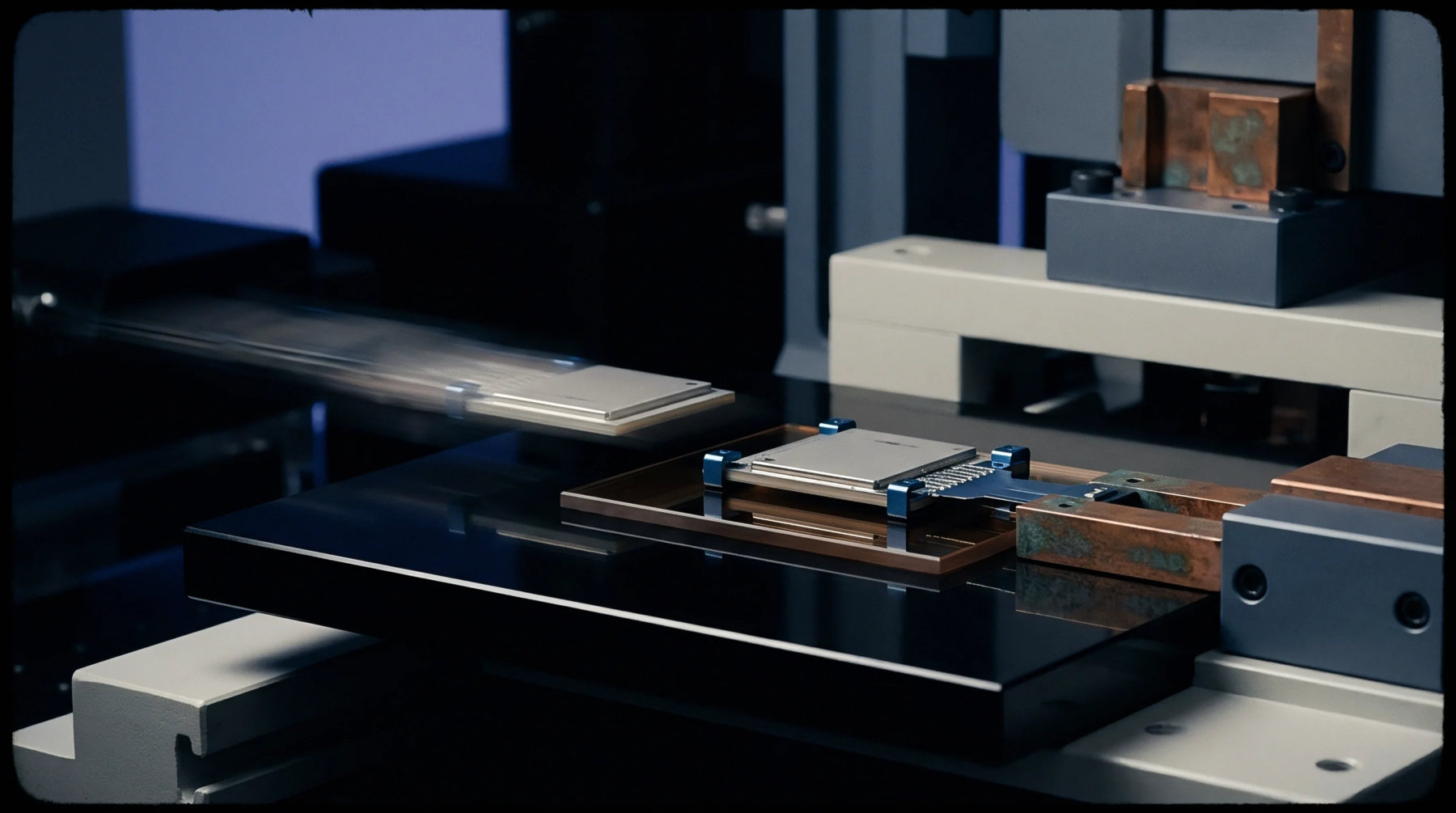
The difference in thermal expansion rates between silicon and circuit board materials can cause solder joints to crack over time. The redistribution layer absorbs a portion of this mechanical stress by acting as a compliant buffer between the die and the board. This buffer extends the operating life of the device by preventing solder joint fatigue during thermal cycling.
Package Integration
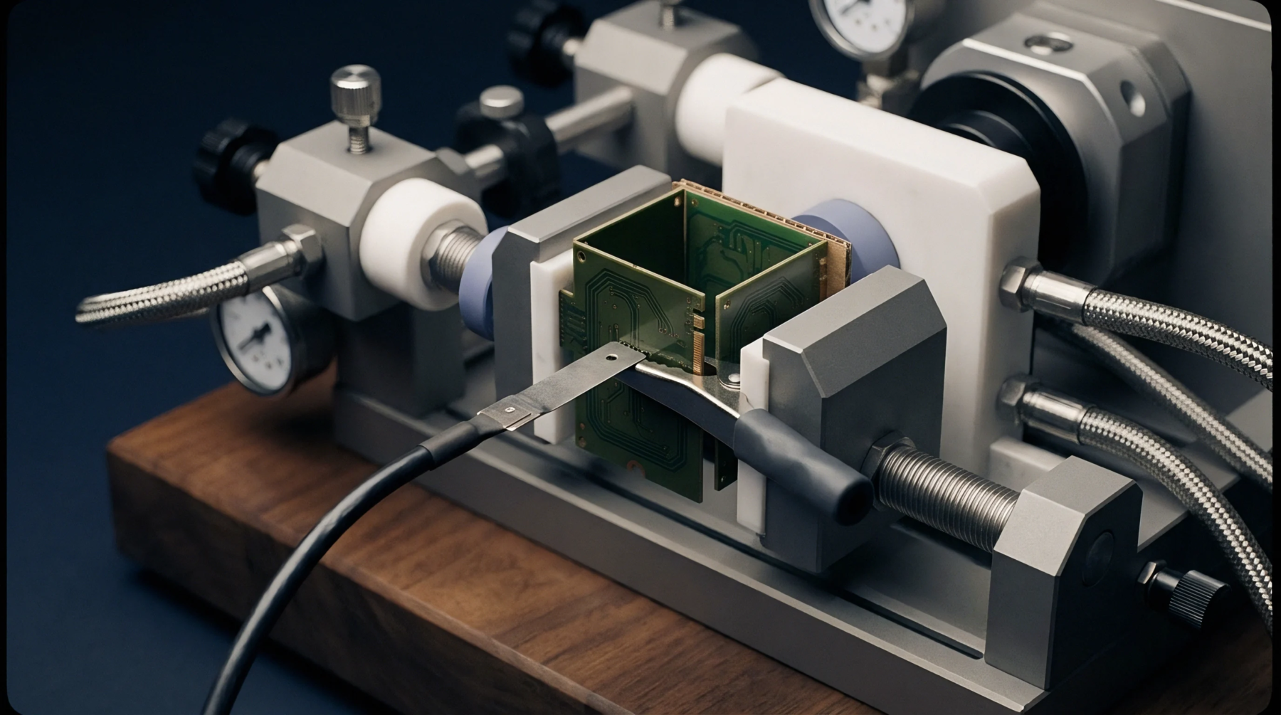
Using this layer allows for the integration of multiple dies into a single high-performance package. The redistribution layer provides the high-speed pathways required for inter-die communication in multi-chip modules. This integration enables higher performance and a smaller footprint for modern smart devices.