Atomic Layer Deposition Passivation Integrity for Sub-GHz Transceiver Crystal Resonators under Pulsed Stress
Atomic layer deposition passivation seals sub-GHz crystal blanks against pulse-induced gas desorption, maintaining clock stability and link margin.

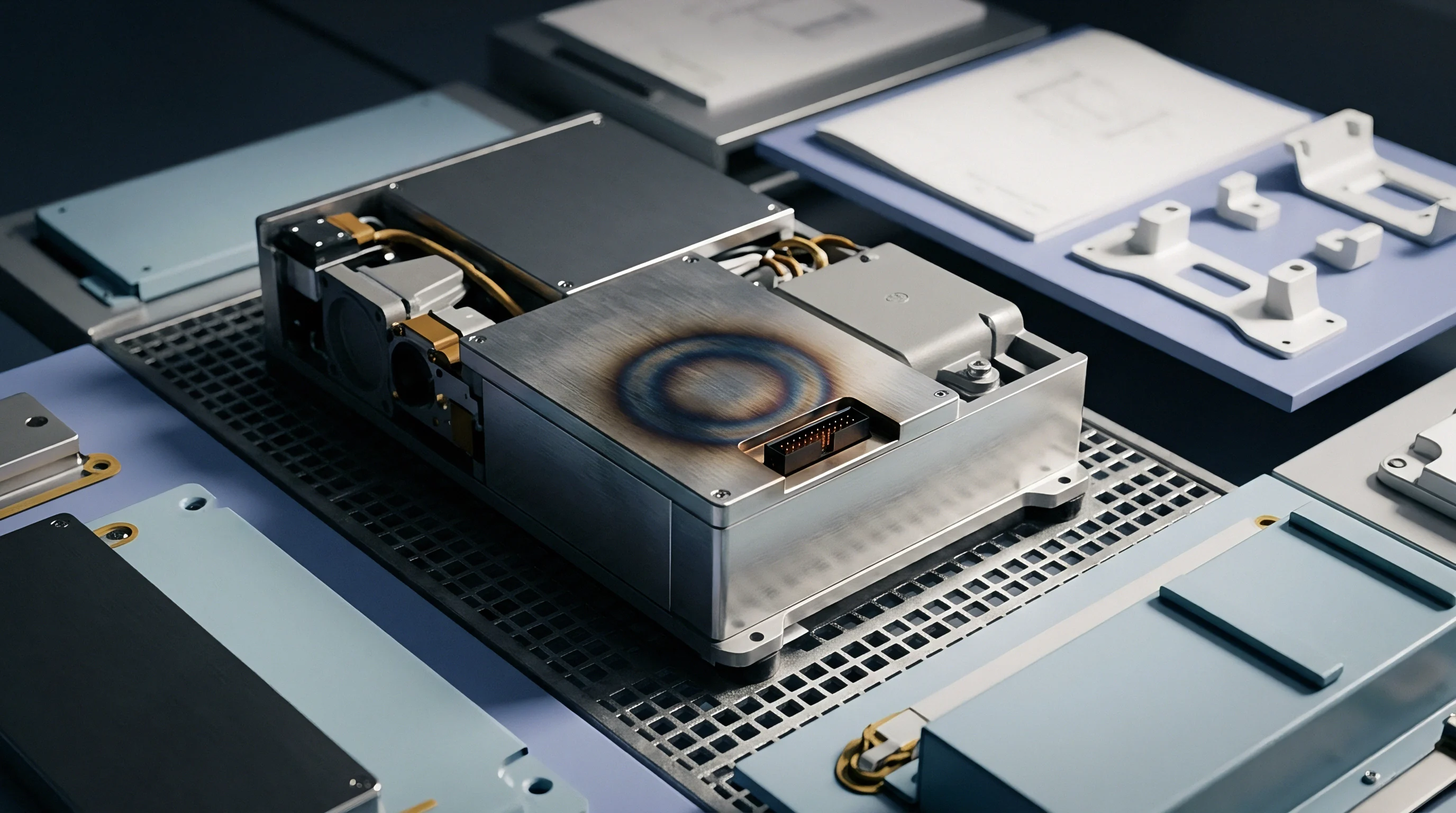
Strain
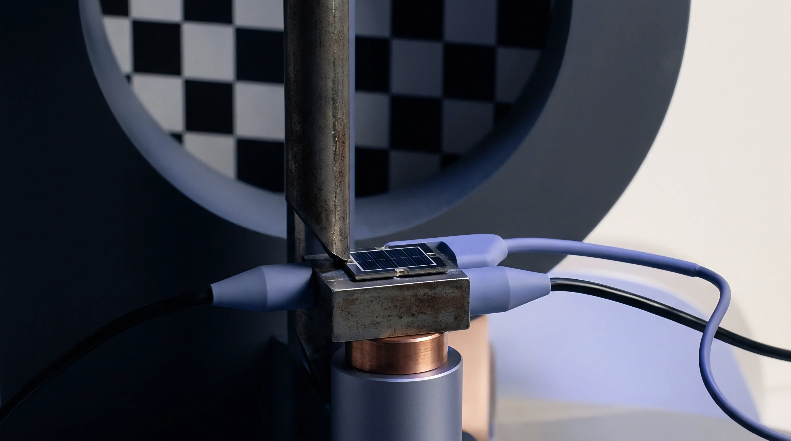
Quartz Crystal Drive Dynamics under High Output Pulsed Transmissions
Industrial, smart-metering, and long-range sub-GHz wireless transceivers frequently fire power amplifier bursts between +20 dBm and +30 dBm. These transmit pulses pull instantaneous supply currents exceeding 100 mA to 500 mA, turning electrical power into mechanical energy inside the AT-cut quartz resonator that serves as the reference clock. Jumping from a microamp-level sleep state to full RF output in tens of microseconds sends a drive current surge across the crystal electrodes, imposing heavy mechanical shear stress on the piezoelectric quartz lattice.
AT-cut blanks operate in thickness-shear mode, with mechanical displacement proportional to the excitation voltage applied across the vacuum-deposited silver or aluminum electrodes.
At these higher drive levels, the crystal resonator enters non-linear vibrational regimes. This drive level dependency creates sudden frequency shifts and transient jumps in equivalent series resistance as RF pulses shock the crystal thermally and mechanically. Over long field deployments, repeated high-amplitude acoustic pulses displace the mechanical lattice enough to weaken the bond between the metal electrodes and the underlying quartz substrate.
For sub-GHz protocols like LoRa, IEEE 802.15.4g SUN, and proprietary narrow-band FSK systems operating with channel spacings down to 12.5 kHz or 25 kHz, even a 5 ppm to 10 ppm reference shift during the preamble degrades carrier tracking, raises packet error rates, and drops frame sync across long links.
Thermal gradients across miniaturized surface-mount packages make these mechanical stresses worse. Compact sub-GHz modules ~ typically 2.0 mm by 1.6 mm or 1.6 mm by 1.2 mm ~ place the quartz element on conductive epoxy pedestals beside the power amplifier IC or power management unit. Direct heat conduction through the package substrate rapidly warms the quartz blank during long transmissions.
Because the thermal expansion coefficients of the quartz matrix, metal electrodes, and ceramic package substrate do not match, shear forces develop along the crystallographic axes, driving transient frequency drift beyond what static TCXO compensation algorithms can clean up.
Surface Contamination and Gas Desorption Mechanisms
Unpassivated quartz blanks keep their microscopic surface roughness, atomic step edges, and trace residues from etching and polishing. Inside standard hermetic packages ~ nitrogen-filled or vacuum-sealed ~ volatile molecules such as water vapor, organic hydrocarbons, and trace oxygen stay adsorbed on the active vibrating surface of the quartz disk. While resting, these adsorbates remain in equilibrium, contributing a baseline mass load accounted for during factory calibration at 25 degrees Celsius.
Pulsed RF operation disrupts that balance. Local thermal dissipation and high acoustic shear velocities inject kinetic energy into the surface, desorbing water and light hydrocarbons from the quartz blank and electrodes. Loss of mass from the vibrating area increases the crystal’s fundamental resonance frequency according to the Sauerbrey equation, which relates surface mass density shifts to fractional frequency changes.
In the subsequent sleep interval, desorbed species readsorb onto the cooling quartz or move toward high-stress electrode interfaces, causing frequency recovery delays and hysteresis. This cycling back and forth creates unpredictable short-term frequency jitter. Over thousands of transmit bursts, repeated thermal and pressure changes inside the package drive chemical reactions between volatile species and the electrodes, oxidizing reactive metals, increasing equivalent series resistance, and permanently lowering the resonator’s quality factor.
Surface Chemistry Passivation via Atomic Layer Deposition
Atomic layer deposition prevents surface instability by building ultrathin, pinhole-free inorganic passivation barriers directly over the quartz blank and its electrodes. Rather than relying on physical or chemical vapor deposition, ALD uses alternating, self-saturating gas-surface reactions. Sub-nanometer thickness control allows uniform coating over complex three-dimensional topographies ~ such as step defects, electrode edges, and ceramic pedestal joints ~ without shifting mechanical resonance parameters or adding appreciable mass to the oscillating crystal.
Sequential vapor exposure of aluminum oxide, titanium dioxide, or silicon dioxide passivates surface hydroxyl groups and dangling quartz bonds. Saturating these bonding sites halts moisture sorption and stops outgassing during mechanical shear. The inert film seals the metal electrode interface, blocking metal migration and oxidation caused by high local electrical fields during transmit bursts.
This stabilizes the acoustic surface impedance of the blank so repeated drive pulses do not induce structural mass shifts or electrode delamination over the component’s operating life.
Atomic layer deposition stops volatile gas desorption from quartz surfaces, maintaining reference clock stability within tight channel allocations during high-power RF transmission bursts.

Structural Failure Modes under Repetitive Mechanical Excitation
Field deployments subject reference crystals in sub-GHz transceivers to millions of transmit stress cycles over several years. Under high acoustic amplitudes and localized thermal transients, unpassivated or inadequately passivated resonators fail in predictable ways.
- Electrode Micro-Delamination Shear forces at the interface between electrode metal and polished quartz exceed bond strength, creating micro-voids that expand into electrode lifting and sharp frequency jumps.
- Acoustic Micro-Cracking High stress at atomic step defects along unpassivated edges causes sub-surface micro-fractures under mechanical cycling, driving up equivalent series resistance and stalling the oscillator.
- Dielectric Film Fracture Coatings subject to thermal expansion mismatches form micro-fissures, giving contaminants access to the underlying quartz and reopening desorption pathways.
- Epoxy Outgassing Accumulation Elevated heat around conductive adhesive pedestals degrades the polymer, releasing gases that condense on the crystal surface and shift fundamental resonance over millions of pulses.
Selecting crystal resonators protected by low-stress atomic layer deposition films insulates the structure against thermal and acoustic fatigue. During early radio qualification trials, transceivers using unpassivated crystal blanks experienced up to 18 ppm total frequency deviation after 500,000 transmit cycles at +27 dBm output power. Adding atomic layer deposition nanofilms kept total drift below 1.5 ppm under identical test conditions, preserving compliance with regional spectral masks without needing software re-calibration loops.
When RF transmit pulse power exceeds +20 dBm in uncompensated sub-GHz transceivers, standard quartz passivation fails, making atomic layer deposition coatings necessary to prevent pulse-induced reference clock drift.

Pinholes

Nanoscale Film Deposition Kinetics and Conformal Coverage Limits
The structural integrity of ALD passivation hinges on binary, self-limiting surface reaction cycles inside a vacuum chamber. Depositing aluminum oxide with trimethylaluminum and water precursors is standard for quartz crystal passivation. Trimethylaluminum gas pulses into the chamber and reacts with surface hydroxyl groups until active sites are consumed.
An inert purge removes excess reactant before water vapor completes the second half-cycle, forming hydroxylated aluminum oxide ready for the next step. Each cycle lays down about 0.1 nanometer of amorphous film, requiring precise exposure times to build coatings between 5 nm and 30 nm thick.
Achieving conformal coverage across the full resonator geometry presents physical difficulties. Features like bevel edges, etch pits, and the vertical steps of screen-printed or sputtered electrodes disrupt molecular diffusion during precursor pulses. Short purges or shadowing can trap unreacted precursor molecules in surface recesses, creating local non-uniformities and intrinsic strain.
If precursor exposure does not fully saturate the surface, pinholes remain where the quartz substrate is left open to the package cavity.
Deposition temperature controls film density and pinhole count. Processing below 150 degrees Celsius produces films with high hydrogen content and incomplete bonding, leaving porous coatings vulnerable to moisture. Conversely, temperatures above 250 degrees Celsius exceed the thermal limits of the conductive epoxies anchoring the blank inside its ceramic housing, prompting pedestal outgassing and mechanical movement.
Balancing this thermal window yields dense, stoichiometric films with dielectric breakdown strength above 7 MV/cm, cutting pinhole density across high-stress zones.
Thermal and Mechanical Stress Degradation in Nanoscale Passivation Coatings
Pulsed operating conditions generate rapid thermal cycles that subject the passivating film to thermo-mechanical strain. Quartz expands anisotropically ~ 13.7 x 10^-6 /K parallel to the a-axis and 7.5 x 10^-6 /K parallel to the c-axis at room temperature ~ while inorganic films like aluminum oxide expand isotropically near 7.0 x 10^-6 /K. During high-power RF transmit bursts, local heating forces differential expansion between the vibrating quartz, metal electrodes, and the overlying coating.
This expansion mismatch generates interface shear stress between the coating and the quartz. Under repeated pulses, micro-cracks form at pinholes or boundary defects and propagate through the dielectric layer. Concentrated stress around pinhole edges accelerates local breakdown, allowing contaminants direct access to the vibrating quartz surface.
Once micro-cracks connect, the passivation coating loses continuity, exposing broader areas of the crystal to outgassing and drive-dependent instabilities.
| Film Chemistry | Deposition Temp (°C) | Refractive Index | Film Stress (MPa) | Pinhole Density (cm^-2) | Dielectric Strength (MV/cm) |
|---|---|---|---|---|---|
| Al2O3 (Thermal) | 200 | 1.65 | +120 (Tensile) | < 0.5 | 8.2 |
| Al2O3 (Plasma) | 120 | 1.61 | -80 (Compressive) | 1.8 | 6.5 |
| TiO2 (Thermal) | 180 | 2.35 | +210 (Tensile) | 3.2 | 4.1 |
| Al2O3 / TiO2 Nanolaminate | 175 | 1.88 | +15 (Balanced) | < 0.1 | 9.0 |
| SiO2 (Plasma) | 150 | 1.46 | -110 (Compressive) | 2.4 | 7.8 |

Pinhole Pinning and Contaminant Ingress Trajectories
Pinholes in passivation films trap residual volatile gases inside the crystal package. Water vapor and hydrocarbons diffuse through pinhole channels via Knudsen diffusion to reach the metal electrode and bare quartz interface. Once inside, contaminants settle into surface energy wells, forming local mass-loading sites that resist normal thermal desorption.
Evaluating atomic layer deposition integrity requires measuring moisture ingress during accelerated stress testing:
- Mount passivated resonators on test fixtures in an environmental chamber at 85 degrees Celsius and 85 percent relative humidity for 500 consecutive hours.
- Apply continuous high-drive RF excitation at +25 dBm equivalent power to induce maximum thickness-shear displacement throughout exposure.
- Measure frequency response curves using an automated network analyzer across drive level sweeps from 1 microwatt to 1000 microwatts every 50 hours.
- Extract equivalent series resistance and frequency jump values to derive drive level dependency hysteresis parameters.
- Perform cross-sectional scanning electron microscopy and energy-dispersive X-ray spectroscopy on failed units to map penetration channels and micro-cracks.
Composite nanolaminates that alternate thin layers of aluminum oxide and titanium dioxide interrupt pinhole propagation. Because pinholes in single layers rarely align across heterogeneous material boundaries, nanolaminates extend diffusion paths for volatile molecules by orders of magnitude. This structure prevents contaminant ingress even if individual sub-layers crack under heavy drive stress.
Nanolaminate coatings formed by alternating dielectric oxide layers disrupt pinhole continuity, maintaining low pinhole density under continuous thermal and mechanical stress.
During qualification testing, brief drive-induced frequency jumps are sometimes attributed to normal initial outgassing within manufacturing tolerances rather than passivation film failure.
Spectra

Frequency Stability and Modulation Degradation under Pulsed RF Stress
Sub-GHz wireless networks rely on stable carriers for spectral efficiency and channel separation. Transceivers running Gaussian Frequency Shift Keying, Phase Shift Keying, or Chirp Spread Spectrum modulation require tight carrier stability to maintain demodulator sensitivity. When high-power PA activation causes dynamic drive shifts in the crystal resonator, the reference pulls off nominal right during preamble transmission.
That transient offset directly erodes link margin. In narrow-band systems operating at 12.5 kHz channel spacing, a 3 ppm shift at 915 MHz creates a 2.745 kHz carrier offset. The signal shifts into adjacent guard bands, causing receiver filter attenuation, corrupted symbol decoding, and battery-draining retransmissions.
In LoRa links, reference instability during a symbol period distorts chirp linearity, raising symbol error rates and cutting receiver sensitivity by 4 dB to 6 dB under weak-signal conditions.
Thermal self-heating inside the transceiver IC compounds the problem. The internal phase-locked loop uses the crystal reference to synthesize operating frequencies. High-frequency phase noise caused by lattice distortion under pulsed stress passes directly into the synthesized local oscillator signal.
This broadens the spectrum, raises adjacent-channel noise floors, and risks non-compliance with regional FCC and ETSI regulatory limits.
What Triggers Phase Noise Jumps under Dynamic Transmit Pulses?
Phase noise jumps in quartz-stabilized local oscillators occur when high excitation levels trigger non-linear mechanical modes in the crystal resonator. Energy delivered by the oscillator drives thickness-shear vibrations into non-linear velocity profiles, coupling the primary resonance to unwanted flexural, extensional, or contour modes. These spurious modes ~ commonly called activity dips ~ shift equivalent electrical parameters over narrow temperature and drive ranges.
Under pulsed RF conditions, jumping from low power to maximum output shifts the effective drive across the electrodes from sub-microwatts to hundreds of microwatts within microseconds. If the crystal blank contains local stress fields, uneven ALD coverage, or unpassivated surface defects, this rapid transition triggers mode coupling. The crystal’s quality factor drops sharply, generating phase noise spikes, sideband regeneration, and carrier phase jitter.
| Band (MHz) | Modulation Scheme | PA Output (dBm) | ALD Passivation | Transmitting Drift (ppm) | Sensitivity Loss (dB) | ESR Jump (%) |
|---|---|---|---|---|---|---|
| 868 | 2-FSK (50 kbps) | +14 | Unpassivated Al | 4.2 | 1.8 | 12.5 |
| 868 | 2-FSK (50 kbps) | +14 | Single Al2O3 (10nm) | 0.8 | 0.2 | 1.1 |
| 915 | LoRa (SF12 / 125kHz) | +22 | Unpassivated Al | 8.7 | 5.4 | 28.0 |
| 915 | LoRa (SF12 / 125kHz) | +22 | Single Al2O3 (10nm) | 1.9 | 0.7 | 3.5 |
| 915 | LoRa (SF12 / 125kHz) | +22 | Nanolaminate (20nm) | 0.4 | 0.1 | 0.3 |
| 920 | GFSK (100 kbps) | +30 | Unpassivated Al | 14.5 | 9.2 | 45.0 |
| 920 | GFSK (100 kbps) | +30 | Nanolaminate (20nm) | 0.9 | 0.3 | 0.8 |
Evaluation of Crystal Drive Level Sweeps and Resonance Parametrics
Evaluating atomic layer deposition integrity requires bench testing with drive level sweeps. A crystal resonator’s equivalent circuit comprises motional inductance, motional capacitance, motional resistance (equivalent series resistance), and shunt capacitance. Under pulsed stress, these parameters must remain stable across the oscillator’s full operating range.
Measuring drive level dependency involves sweeping excitation power across four orders of magnitude while recording impedance curves on an RF impedance analyzer or crystal test system:
First, the crystal sits in a temperature-controlled fixture tied to an automated network analyzer. Drive power sweeps from 0.01 microwatts to 1000 microwatts in logarithmic steps at 25 degrees Celsius while measuring fundamental series resonance frequency, parallel resonance frequency, and equivalent series resistance. Unpassivated resonators exhibit sharp resistance spikes and frequency drops ~ negative drive level dependency ~ at low drive levels due to surface contamination barriers.
Dense ALD coatings maintain flat resistance profiles across the entire sweep.
Second, the drive sweep repeats while stepping package temperature using thermoelectric coolers. Temperature cycles from -40 degrees Celsius to +85 degrees Celsius at 10 degrees Celsius per minute while the oscillator delivers maximum-power pulses. This thermo-mechanical stress exposes activity dips, hysteresis loops, and non-linear frequency offsets caused by strain in the coating or interface defects.
Checking oscillator stability under pulsed stress involves specific parametric limits:
- Equivalent Resistance Shift Check Motional resistance variation must stay under 5 percent across the drive spectrum from 1 microwatt to 500 microwatts.
- Resonance Hysteresis Sweep Frequency curves captured during ascending drive sweeps must match descending sweeps within 0.5 ppm.
- Spurious Mode Suppression Map Unwanted mechanical modes must remain at least 15 dB below the fundamental thickness-shear peak across all operating temperatures.
- Phase Noise Floor Verification Phase noise at a 10 kHz offset from the carrier must degrade by no more than 3 dB during high-power PA switching transients.
Whether ALD-passivated crystals can maintain sub-ppm frequency alignment over a 20-year deployment under extreme thermal cycling without periodic software compensation remains an open question.
Fatigue

Long-Term Aging Kinetics and Stress Acceleration Models
Crystal aging is the permanent drift of fundamental resonance frequency over time. In sub-GHz transceivers, long-term drift stems from two primary mechanisms: mass transfer via surface outgassing or contaminant adsorption, and stress relief within the quartz blank, metallization, and passivation layers. High-power transmit pulses accelerate both processes by dumping kinetic and thermal energy directly into the active vibrating area.
Standard aging models follow logarithmic kinetics, expressing cumulative frequency drift Delta_f over initial frequency f0 as:
Delta_f / f0 = A ln(1 + B t)
Here, A is the aging rate amplitude factor, B is the time scaling constant, and t is elapsed operating time. Under quiet conditions, A remains low, driven by slow ambient diffusion. Under pulsed stress, high acoustic velocity and thermal shock elevate A, accelerating aging and pushing frequency drift past lifetime limits within months.
Accelerated life testing relies on Arrhenius kinetics to project multi-year aging from high-temperature and drive-stress exposures. The acceleration factor depends on the activation energy of the primary degradation mechanism ~ typically 0.4 eV to 0.8 eV for desorption and stress relief in quartz. Subjecting crystals to elevated temperatures while running continuous maximum-power RF pulses accelerates mechanical fatigue, revealing defect growth, film embrittlement, and interface failures within short test windows.
Mechanical Interfacing and Package Stress Interplay
The internal mounting structure transfers significant stress to the quartz blank. Blanks rest on conductive epoxy pedestals anchored to ceramic substrate pads, which provide mechanical support and electrical contact to the electrodes. Under pulsed stress, thermal gradients across the package create bending moments at these mounting points.
If the ALD coating covers the conductive epoxy joints without stress buffering, strain concentrates where rigid metal oxide meets flexible polymer adhesive. Thermal cycling causes micro-cleavage along this boundary, sending cracks along the electrode tracks. This increases contact resistance, introduces phase noise, and causes non-linear frequency shifts during power amplifier pulses.
Minimizing mechanical strain requires matching the compliance of the passivation coating to the package materials. Nanolaminate architectures that alternate soft, amorphous layers with dense dielectric barriers relieve residual film stress. Engineered properly, nanolaminates retain sufficient flexibility to absorb shear strain at the epoxy pedestals without cracking or peeling.
Standard ISO 17025 qualification protocols require continuous RF pulse stress testing to validate crystal frequency stability before approving modules for field deployment.
Quantification of Operational Failure Costs
Ignoring crystal fatigue under pulsed stress creates operational and financial risks in large sub-GHz networks. When reference clock drift exceeds a receiver node’s capture bandwidth, devices lose connectivity, driving manual service calls, component replacements, or complete network reconfigurations.
In utility metering infrastructure, where endpoints must operate unattended for 15 to 20 years on lithium thionyl chloride batteries, crystal failures undermine project economics. Excessive clock drift forces transceivers to lengthen preambles and widen receiver windows to maintain synchronization, raising sleep current and reducing battery life from 15 years to under 5. Field replacement costs quickly swamp any upfront savings from unpassivated or poorly passivated crystals.
Deploying sub-GHz modules with unpassivated crystal resonators in high-power transmit applications leads to field failures, battery drain, and network collapse across industrial links.
Dossier
Procurement Specifications for High-Integrity Crystal Resonators
Procuring crystal resonators for high-power sub-GHz transceivers requires looking past basic datasheets. Standard datasheets specify frequency tolerance at 25 degrees Celsius and stability over temperature, but omit drive level dependency hysteresis, aging under pulsed stress, and passivation parameters. Procurement specifications must define explicit material requirements, deposition standards, and stress verification protocols to ensure long-term field reliability.
Technical specifications provided to suppliers must define the ALD passivation architecture. Sourcing documentation should mandate conformal dielectric coatings applied directly over the polished blank and metal electrodes before hermetic package sealing. Manufacturers should be required to provide cross-sectional electron microscopy demonstrating uniform thickness, low pinhole density, and stoichiometric composition across production lots.
Procurement contracts should establish strict acceptance limits for drive level dependency and pulsed stress behavior. Testing must evaluate performance before and after high-drive exposure, rejecting lots with parameter shifts beyond specified thresholds. Explicit component specifications prevent substitution of lower-grade, unpassivated blanks during high-volume production runs.
| Parameter | Test Condition | Standard Crystal Bound | ALD Passivated Bound | Unit |
|---|---|---|---|---|
| Frequency Tolerance | 25°C, 10 µW drive | ± 10 | ± 10 | ppm |
| Frequency Stability | -40°C to +85°C | ± 20 | ± 10 | ppm |
| Drive Level Dependency (DLD) | 0.01 µW to 500 µW sweep | < 5.0 | < 0.5 | ppm |
| Max Motional Resistance (ESR) | Fundamental mode, 25°C | < 60 | < 40 | Ω |
| ESR Jump under Pulsed Stress | 500k pulses @ +27 dBm | < 25.0 | < 2.0 | % |
| Post-Stress Aging (1 Year) | Accelerated at 85°C | ± 3.0 | ± 0.5 | ppm |
| Passivation Layer Integrity | 85°C / 85% RH, 500 hrs | Unspecified | Zero micro-cracks | Visual / SEM |

Vendor Qualification and Quality Audit Frameworks
Auditing crystal manufacturing facilities requires evaluating cleanroom conditions, deposition tool calibration, and in-line process controls. Atomic layer deposition demands strict vacuum control and precursor dosing. Quality audits should verify that production lines use automated ellipsometry and X-ray photoelectron spectroscopy to track film thickness and stoichiometry lot by lot.
Audit frameworks must also evaluate the supplier’s stress-testing capabilities. Reputable vendors maintain reliability labs equipped with automated RF pulse benches, drive sweep analyzers, and environmental shock chambers. Auditors should verify that suppliers perform continuous burn-in tests on sample units from every wafer batch to catch defects before assembly.
Full component traceability is critical during vendor qualification. Suppliers must trace finished surface-mount units back to the original quartz ingot, polishing batch, electrode metallization run, and ALD deposition cycle. When field failures occur, complete lot histories enable engineering teams to isolate affected batches and identify the root process deviation.
Embedding these qualification protocols into sourcing protects sub-GHz hardware from premature degradation. Sourcing passivated crystals backed by test data preserves carrier stability, maintains link budgets, and ensures multi-year operational life in demanding infrastructure.
Procurement specifications that include ALD film parameters prevent component substitution and ensure long-term clock stability under pulsed transmit conditions.
A standard procurement specification clause reads: “The supplier shall certify that all delivered crystal resonators feature an inorganic atomic layer deposition passivation layer protecting the quartz blank and metal electrodes, holding drive level dependency frequency shifts below 0.5 ppm after 500,000 pulsed RF excitation cycles at maximum rated output power.”