Non-Volatile Memory Charge Retention Mechanics under High-Temperature Industrial Environments
High thermal stress accelerates floating node leakage via Poole-Frenkel emission and trap-assisted tunneling, requiring Grade 0 silicon and active firmware refresh.
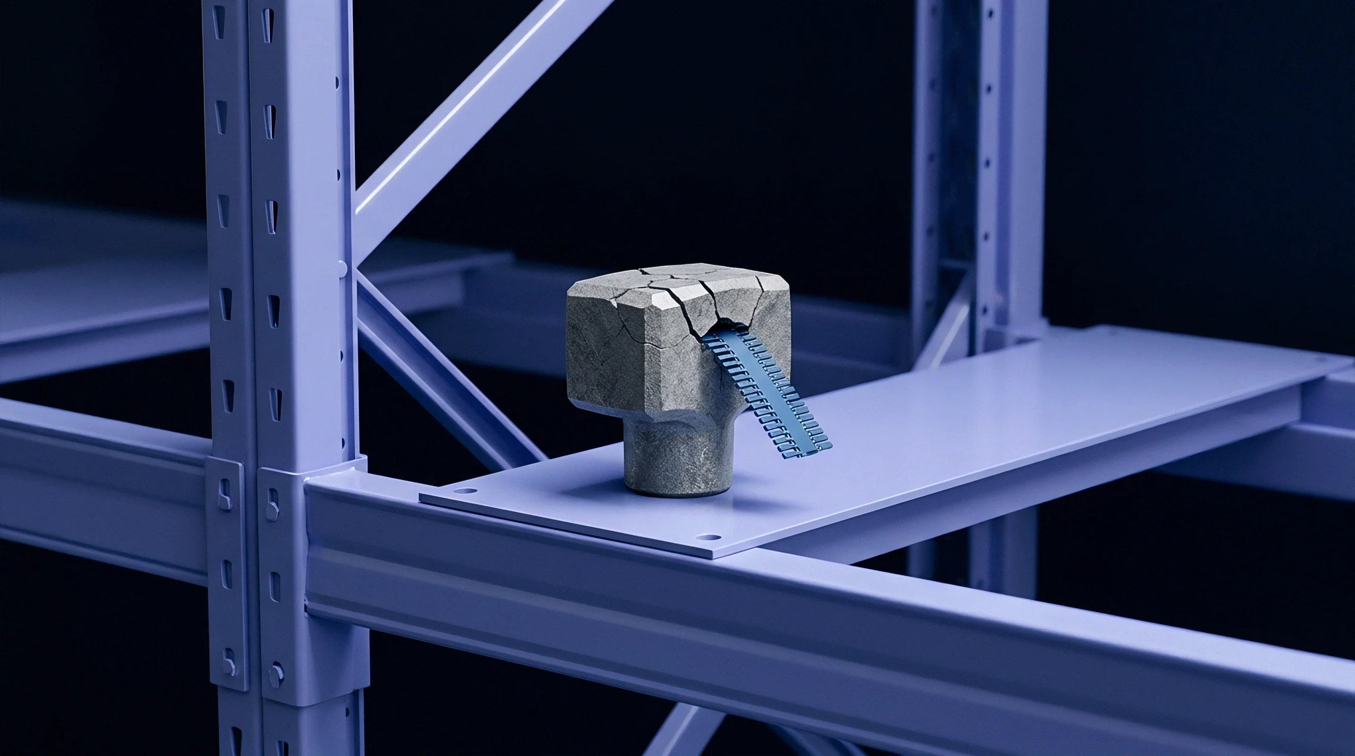
Barrier
Non-volatile memory cells in high-temperature industrial modules store electronic charge on polysilicon nodes encased in silicon dioxide insulation. Physical confinement depends on dielectric potential barriers that keep trapped carriers from leaking into the substrate. At ambient temperatures between 125°C and 175°C, thermal energy enters the crystal lattice and pushes electrons toward the conduction band.
Thermal excitation then combines with electric field stress, changing retention mechanics and compromising charge traps.
Ambient heat lowers the effective potential barrier surrounding the storage node. As temperatures climb, thermal agitation broadens the energy distribution of stored electrons, making it more likely that carriers gain enough energy to clear the barrier wall. Negative charge then leaks from the floating gate or nitride traps into the substrate or control gate, driving the programmed threshold voltage back toward an erased state.
This discharge degrades data in unpowered radios, edge controllers, and sensor modules.
Thermionic emission drives much of this charge loss at high temperatures. Electrons in the floating gate’s energy well absorb thermal energy from the lattice, climbing the potential barrier at the silicon dioxide boundary. Emission rates scale exponentially with temperature and inversely with barrier height.
At room temperature, barriers near 3.1 electron-volts keep charge isolated for decades. Once junction temperatures pass 150°C, thermionic emission speeds up by several orders of magnitude, causing measurable cell degradation within weeks.

Floating Gate Charge Storage Dynamics
At normal operating temperatures, electrons injected into a polysilicon island stay trapped behind high potential walls. Storing charge on this isolated conductor raises the threshold voltage needed to turn on the underlying transistor channel. Under continuous heat, however, charge inside the floating gate redistributes toward equilibrium.
Electrostatic repulsion pushes stored electrons closer to the oxide interface, concentrating local field strength across thin tunnel dielectrics.
This field concentration accelerates leakage. Stored negative charge creates a self-induced electric field that resists retention, forcing carriers toward the oxide boundary where thermal energy lets them bypass the dielectric thickness through field-assisted routes. Over time, cell threshold voltages drift downward, eroding the read margin between logic states until sense amplifiers start misreading stored bit patterns.

Thermal Activation and Quantum Tunneling Mechanics
Thermal lattice vibrations impart kinetic energy to trapped electrons. Quantum mechanical tunneling through gate oxides takes the form of direct tunneling when dielectrics are under three nanometers thick, or Fowler-Nordheim tunneling under strong electric fields. High operating heat excites electrons into higher energy sub-bands of the floating gate conduction band, shortening the physical distance carriers must tunnel through the trapezoidal barrier.
Between 125°C and 175°C, thermally assisted tunneling becomes the dominant loss path. Electrons do not need enough energy to jump the full oxide conduction band edge; partial thermal excitation lets them tunnel through the narrower upper slice of the barrier. This hybrid mechanism cuts retention lifespans far below what room-temperature tunneling models predict.
Continuous operation at 150°C accelerates electron leakage through thin gate oxides, reducing unrefreshed data retention from ten years down to twenty-two days.
Trap-assisted tunneling speeds up charge loss when structural defects enter the gate oxide. Manufacturing impurities, program-erase cycles, and thermal stress produce defect sites throughout the silicon dioxide network. These intermediate energy levels work like stepping stones, letting electrons hop from trap to trap instead of crossing the barrier in one jump.
High temperatures increase trap occupancy and phonon-assisted hopping efficiency, breaking down charge isolation.

Bandgap Degradation under Continuous High Heat
Dielectrics degrade structurally under prolonged heat. Silicon dioxide has a nominal energy bandgap near 9 electron-volts at room temperature, but thermal expansion narrows it during high-temperature operation. That narrowing lowers the conduction band offset between the silicon substrate and the dielectric, shrinking the barrier height facing stored electrons.
Charge Trap Flash architectures sandwich silicon nitride between silicon dioxide layers to hold electrons in localized states. Localized trapping keeps a single oxide defect from draining an entire node. High thermal stress, though, excites trapped carriers laterally through the nitride layer.
As stored electrons shift position inside the trapping film, internal field profiles change and threshold voltages drift across the array.
| Mechanism | Dominant Temp Range | Activation Energy Range | Oxide Thickness Dependency | Primary Degradation Effect |
|---|---|---|---|---|
| Thermionic Emission | 140°C to 200°C | 1.1 eV to 1.3 eV | Independent of thickness | Unassisted charge escape over potential barrier |
| Thermally Assisted Tunneling | 100°C to 150°C | 0.6 eV to 0.9 eV | Inverse linear with thickness | Carrier tunneling through upper barrier edge |
| Trap-Assisted Tunneling | 85°C to 175°C | 0.3 eV to 0.5 eV | Exponential with defect density | Hopping conduction across dielectric defects |
| Poole-Frenkel Conduction | 125°C to 185°C | 0.7 eV to 1.0 eV | Strong electric field dependency | Field-enhanced thermal ionization of deep traps |
Heat degrades stored potential, pushing charge leakage up exponentially as thin oxides fail first. Floating gate cells lose charge faster than localized charge trap nodes because conductive polysilicon lets stored carriers drain through any single breakdown path. Localized nitride traps retain charge away from local oxide flaws, but high temperatures still drive thermal detrapping out of deep wells into shallow band edges.
Without periodic refresh cycles, stored potential eventually drains entirely.
What specific electron transition state governs the transition between trap-assisted hopping and thermionic emission when junction temperatures cross 165°C?

Lattice
Lattice perfection within silicon substrates and oxide dielectrics controls long-term charge retention. High operating temperatures introduce mechanical stress and atomic displacements inside memory arrays. Because silicon wafers, polysilicon gates, metal interconnects, and silicon dioxide layers expand at different rates, mechanical strain builds across material interfaces, breaking silicon-oxygen bonds and generating point defects and dangling bonds that ruin energy barriers.
Defects accumulate faster under long duty cycles at elevated temperatures. Continuous heat creates high concentrations of interface traps (Nit) and fixed oxide charges (Qf) at silicon dioxide boundaries. These interface states introduce energetic levels within the forbidden bandgap, acting as generation-recombination centers that skew electrostatic field distributions across memory transistors.
Poole-Frenkel emission creates a major defect-driven leakage path through damaged dielectrics. Electrons trapped in neutral oxide defects undergo field-assisted thermal ionization. Heat lowers the energy required to ionize these trapped carriers into the dielectric conduction band, driving up Poole-Frenkel current and turning insulating oxide layers into weak conductors during long industrial deployments.

Poole-Frenkel Emission Dynamics
Internal electric fields in scaled flash cells exceed three megavolts per centimeter during normal operation. These strong fields distort the coulombic potential wells of lattice defects, lowering barrier walls in the direction of the field. Thermal energy then kicks trapped electrons out of these shallow wells into the oxide conduction band, where they drift freely under the electric field.
Defect density directly determines the magnitude of Poole-Frenkel conduction. High temperatures accelerate atomic diffusion inside the dielectric, driving mobile impurity ions like sodium and hydrogen toward oxide interfaces. As these ions accumulate near the floating gate boundary, they distort potential profiles and concentrate local electric fields ~ spurring higher Poole-Frenkel emission in a feedback loop that speeds up discharge.
Interface Trap Generation Mechanics
Dangling bonds at the boundary between single-crystal silicon and amorphous silicon dioxide determine interface trap density. Unpassivated atomic sites capture or release electrons based on local Fermi energy levels. High temperatures break hydrogen-passivated silicon bonds, freeing atomic hydrogen and leaving raw interface states behind that shift threshold voltages and accelerate array decay.
This interface state growth shifts threshold voltages over operational lifespans. Programmed cells lose negative threshold margins as positive charge builds in donor-like interface states near the substrate. Erased cells drift in the opposite direction, compressing read margins from both ends and increasing raw bit error rates during high-temperature operation.
Silicide and Oxide Interfacial Microcracking
Thermal cycling between ambient cold and operational heat causes differential expansion across the IC stack. Silicide layers on low-resistance gate contacts expand at different rates than the underlying polysilicon and inter-layer dielectrics. Repeated thermal stress eventually generates microcracks and lattice dislocations that propagate through thin gate oxides.
Microcracks at interfaces create direct paths for leakage. Structural dislocations alter local band structures, narrowing the bandgap along crack boundaries so electrons flow through high-dislocation channels at lower activation energies than in pristine oxide. Arrays under persistent expansion stress undergo localized retention failures long before standard dielectric wear-out models predict.
- Stress-Induced Leakage Current Low-energy traps created during program-erase cycles allow continuous direct tunneling through damaged dielectrics at standard operating voltages.
- Thermal Detrapping Drift Deep energy trap states release charge under sustained heat, shifting localized threshold voltages in charge-trap architectures.
- Interface State Generation Broken silicon-hydrogen bonds at the oxide boundary leave dangling bonds that capture mobile carriers and collapse read margins.
- Mobile Ion Migration Alkali contamination ions drift across dielectric layers under internal electric fields, distorting local potential profiles.
Dielectric degradation shifts noticeably above 125°C junction temperature. While stress-induced leakage current (SILC) dominates low-temperature wear after program-erase cycling, high-temperature operation causes thermal detrapping and Poole-Frenkel emission to take over, discharging floating nodes regardless of prior endurance history. Unused written arrays lose stored data under severe heat almost as quickly as heavily cycled ones.
| Defect Type | Physical Origin | Energy Level Below Oxide Conduction Band | Cross-Section Area | Thermal Recovery Temp |
|---|---|---|---|---|
| E’ Center Trap | Oxygen vacancy in silicon dioxide | 3.1 eV | 10⁻¹⁵ cm² | 300°C |
| Interface State (Nit) | Unpassivated silicon dangling bond | 0.3 eV to 0.8 eV | 10⁻16 cm² | 220°C |
| Non-Bridging Oxygen | Broken silicon-oxygen network bond | 1.8 eV to 2.2 eV | 10⁻14 cm² | 250°C |
| Hydrogen Trap Center | Radiative or thermal bond cleavage | 1.2 eV | 10⁻¹⁷ cm² | 150°C |
Silicon degrades under sustained stress as leakage pathways spread across defect-rich dielectric boundaries during high-temperature exposure. Retention is evaluated by tracking threshold voltage shifts across test arrays baked in environmental chambers; elevated thermal audits show a 14 millivolt threshold shift per thousand hours across 150°C test batches.
High ambient temperature drives charge out of floating nodes far faster than dielectric wear alone predicts.
Interface trap generation does not saturate after initial high-temperature bake-in; empirical test data shows continuous defect growth during active field deployment, explaining early threshold failures in Grade 0 modules.

Bench
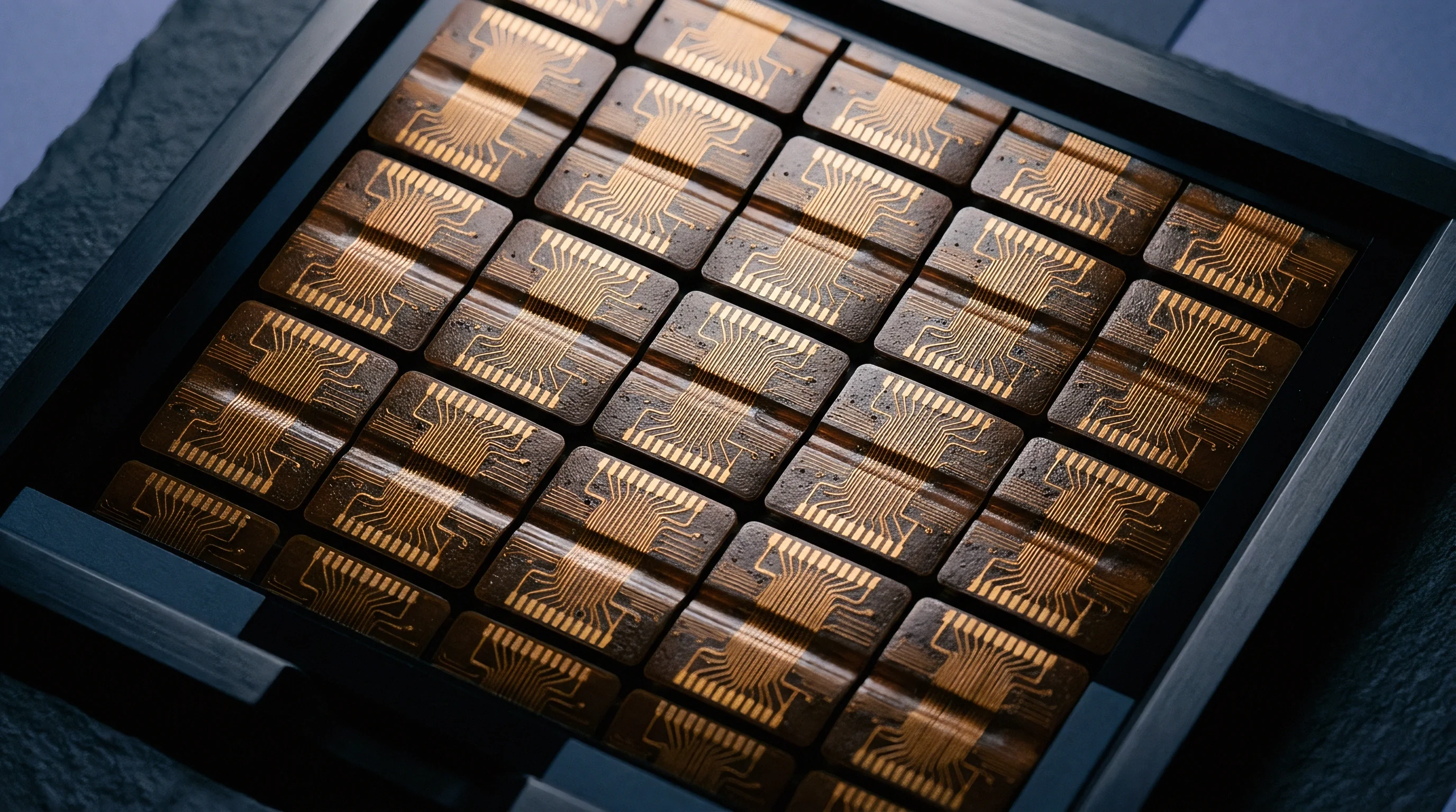
Validating non-volatile memory charge retention relies on qualification protocols that simulate years of field exposure within laboratory timelines. High-temperature bake testing serves as the baseline: memory chips are fully programmed across all address spaces, placed unpowered in thermal chambers between 150°C and 250°C, and read at scheduled intervals to measure charge loss rates over time.
Arrhenius kinetic models convert short-term bake results into projected lifespans at lower operating temperatures. The classical Arrhenius equation calculates an acceleration factor (AF) from target operating temperature, stress bake temperature, Boltzmann’s constant, and an assumed constant activation energy (Ea). Standard automotive and industrial procedures typically set fixed activation energy values between 1.1 eV and 1.3 eV for floating gate modeling.
These qualification assumptions fail when applied to deep-submicron nodes in harsh environments. Effective activation energy does not stay constant across all thermal regimes because multiple leakage mechanisms operate at once, each driven by its own activation energy. Extrapolating lifespan projections from a single assumed activation energy yields unrealistically optimistic reliability estimates.

High Temperature Bake Qualification Procedures
High Temperature Storage Life (HTSL) testing per JESD22-A103 demands tight chamber temperature control. Devices are written with specific pattern topologies ~ solid ones, solid zeros, and checkerboards ~ to isolate row and column interference leakage. Readout runs occur at room temperature after thermal exposure periods of 168 hours, 500 hours, and 1,000 hours.
Evaluating results requires tracking threshold voltage distributions across millions of cells on a test die. Broadened distribution tails highlight isolated weak cells that lose charge up to ten times faster than the array median. Because standard qualification specs pass lots based on median retention metrics, high-temperature installations remain vulnerable to early corruption in tail cells.
Where Does Arrhenius Derivation Fail under Industrial Thermal Cycling?
Linear Arrhenius extrapolation assumes one physical failure mechanism dominates at both stress test temperatures and field operating conditions. Elevating bake temperatures to 200°C to compress testing from months into days makes thermionic emission the primary discharge path, producing a high apparent activation energy near 1.2 eV. At actual industrial operating temperatures between 125°C and 150°C, trap-assisted tunneling and Poole-Frenkel conduction govern charge leakage with activation energies of only 0.4 eV to 0.7 eV.
Extrapolating 200°C test data down to 125°C using an assumed 1.1 eV activation energy overstates retention lifespans by up to two orders of magnitude. The leakage mechanism actually active at 125°C drains charge much faster than high-temperature thermionic models predict, meaning standard test procedures miss low-activation-energy paths that cause field radios operating continuously above 135°C to fail.
- Program test memory arrays with worst-case data patterns, including inverse checkerboard configurations, at room temperature.
- Measure baseline threshold voltage distributions across all array sectors via direct memory controller test interfaces.
- Expose unpowered memory units to 175°C bake conditions inside calibrated environmental chambers for 500 continuous hours.
- Perform full read verification on cooled units at 125°C to measure threshold voltage shift tails under operational thermal bias.
- Calculate multi-point activation energy spectra by repeating thermal bakes at 150°C and 200°C across independent sample lots.
Arrhenius models break down as thermal stress curves bend downward at high temperatures. Rigorous qualification requires multi-mechanism extraction methods rather than single-point activation energy assumptions; mapping the full activation energy spectrum across the operating range is necessary to prevent field failures that standard tests miss.
Activation Energy Extraction Errors
Single-point temperature testing introduces significant estimation errors into reliability dossiers. Measuring data loss at only one stress temperature forces dependence on theoretical activation energy figures from vendor datasheets, even though real activation energy varies with die fabrication options, nitridation profiles, and prior program-erase endurance wear.
Multi-temperature profiling measures charge decay across three or more bake temperatures. Plotting log leakage rates against inverse absolute temperature produces slope curves whose gradients reveal true local activation energies. Curve inflections highlight where dominant leakage mechanisms transition from trap-assisted tunneling to thermionic emission, setting safe acceleration limits for specific silicon batches.
| Stress Temp (°C) | Assumed Ea (eV) | Calculated AF (vs 125°C) | Equivalent Hours at 125°C | Actual Measured AF (Multi-Mechanism) |
|---|---|---|---|---|
| 150 | 1.1 | 7.8× | 7,800 | 3.2× |
| 175 | 1.1 | 51.2× | 51,200 | 11.4× |
| 200 | 1.1 | 288.5× | 288,500 | 34.1× |
| 225 | 1.1 | 1,420.0× | 1,420,000 | 89.6× |
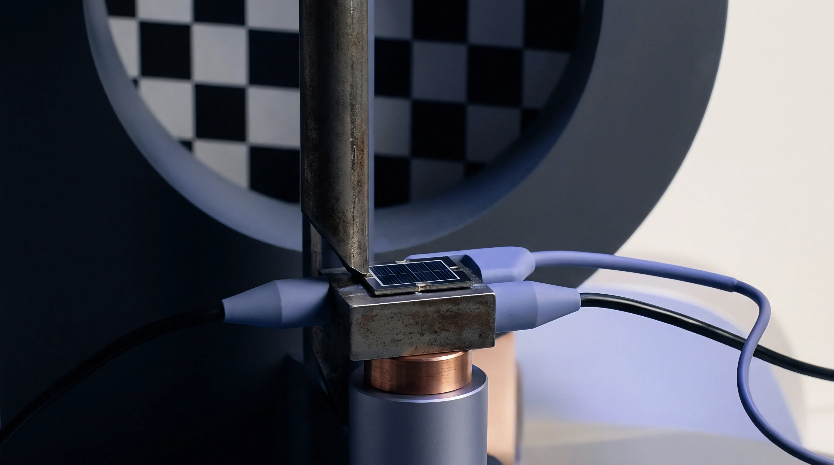
On the bench, isolating leakage currents requires bypassing on-chip regulators during thermal stress testing. Test data collected from 175°C bakes frequently misleads procurement teams when standard single-point Arrhenius models are applied and margins collapse under heat.
Section four of JESD22-A108 dictates bake times at 150°C that fail to catch trap-assisted thermal leakage occurring above 175°C.
A twenty-eight thousand dollar re-qualification outlay resulted from relying on vendor-supplied single-point bake data that predicted ten-year retention at 135°C, only to discover field nodes experiencing total byte corruption within eighteen months of continuous operation inside engine control housings.


Protocol
Mitigating charge degradation requires memory controller protocols that operate dynamically inside high-temperature modules. Relying solely on oxide insulation fails when ambient temperatures remain above 125°C for years. Instead, software algorithms, controllers, and system firmware must work together to detect, correct, and refresh decaying storage cells before raw bit errors exceed ECC limits.
Autonomous memory scrubbing runs background read routines across storage blocks during system idle windows. The controller reads stored sectors, passes payloads through hardware error-correcting code (ECC) engines, and checks for bit errors caused by thermal charge loss. When error counts on a page cross warning thresholds, the controller rewrites that page to a fresh block, restoring full charge levels to floating gate nodes.
Memory scrubbing introduces operational trade-offs in energy-constrained radio modules. Active scrubbing requires array reads, ECC decoding, and block erase-rewrite operations that draw milliamperes of supply current. In battery-powered IoT transceivers, running refresh routines too frequently shortens operating lifespan, forcing architects to balance retention safety against overall battery budgets.

Autonomous Controller Scrubbing Intervals
Scrubbing frequency dictates data preservation in high-temperature storage elements. Static scrub intervals fixed at boot risk data loss if ambient temperatures spike during plant operation. Advanced controllers integrate thermal sensors, scaling scrub frequencies dynamically in response to real-time junction temperature readings.
Scrubbing intervals scale exponentially with reported temperatures. At 85°C, a controller might execute background memory scrubs once every thirty days; if sensors report sustained junction temperatures of 150°C, it accelerates the scrub loop to run every forty-eight hours. Because scrubbing draws operational current, controllers must adjust power modes dynamically to preserve baseline reliability.

Error Correction Code Overhead Metrics
Hardware error correction serves as the main defense against thermal charge loss between refresh cycles. Single Error Correction, Double Error Detection (SECDED) Hamming codes add eight parity bits per sixty-four-bit word to fix single-bit inversions from tail-cell leakage. High-temperature industrial environments require stronger schemes, such as Bose-Chaudhuri-Hocquenghem (BCH) or Low-Density Parity-Check (LDPC) algorithms, capable of resolving four to eight random bit errors per kilobyte page.
ECC implementations carry silicon area, memory capacity, and latency penalties. High-capability LDPC engines require complex matrix decoding logic, adding die area and extending read latency by several clock cycles per access. Parity storage also consumes 10% to 25% of net flash capacity, driving up effective cost per megabit.
Designers must balance parity overhead against target operating temperatures and field deployment targets.

Cell Wear Distribution Algorithms
Continuous scrubbing and block refreshes add endurance wear to thermal-stressed arrays. High heat accelerates oxide trap generation during program and erase operations, cutting maximum write endurance from 100,000 cycles to under 5,000 cycles at 150°C. Wear-leveling algorithms prevent localized block wear-out caused by aggressive refresh protocols.
Wear-leveling controllers track erase cycle counts across physical blocks. Static wear-leveling rotates low-turnover code, like bootloader binaries, into heavily cycled sectors so the die degrades uniformly. In high-temperature environments, retention-aware algorithms also bypass sectors that showed high baseline thermal leakage during initial qualification.
- Dynamic Scrub Scaling System controllers must adjust memory refresh intervals using real-time junction temperature feedback.
- High-Margin ECC Engine Controllers in Grade 0 operating environments require at least eight-bit error correction per 512-byte sector.
- Retention-Aware Wear Leveling Firmware memory managers should rotate static binary payloads out of sectors displaying high baseline leakage.
- Power Budget Allocation System power architectures need dedicated battery capacity set aside specifically for high-temperature memory scrubs.
Errors accumulate over time, requiring controllers to run scrub loops to maintain data integrity across thermal peaks. Continuous drift occurs when nodes operate above 135°C on factory floors without active background refresh routines enabled in firmware.
Memory scrub cycles consume battery capacity that radio designers reserved for RF transmission margins.
Background memory refresh intervals scale exponentially with junction temperature, doubling execution frequency for every ten-degree Celsius rise above baseline industrial thresholds.

Ledger
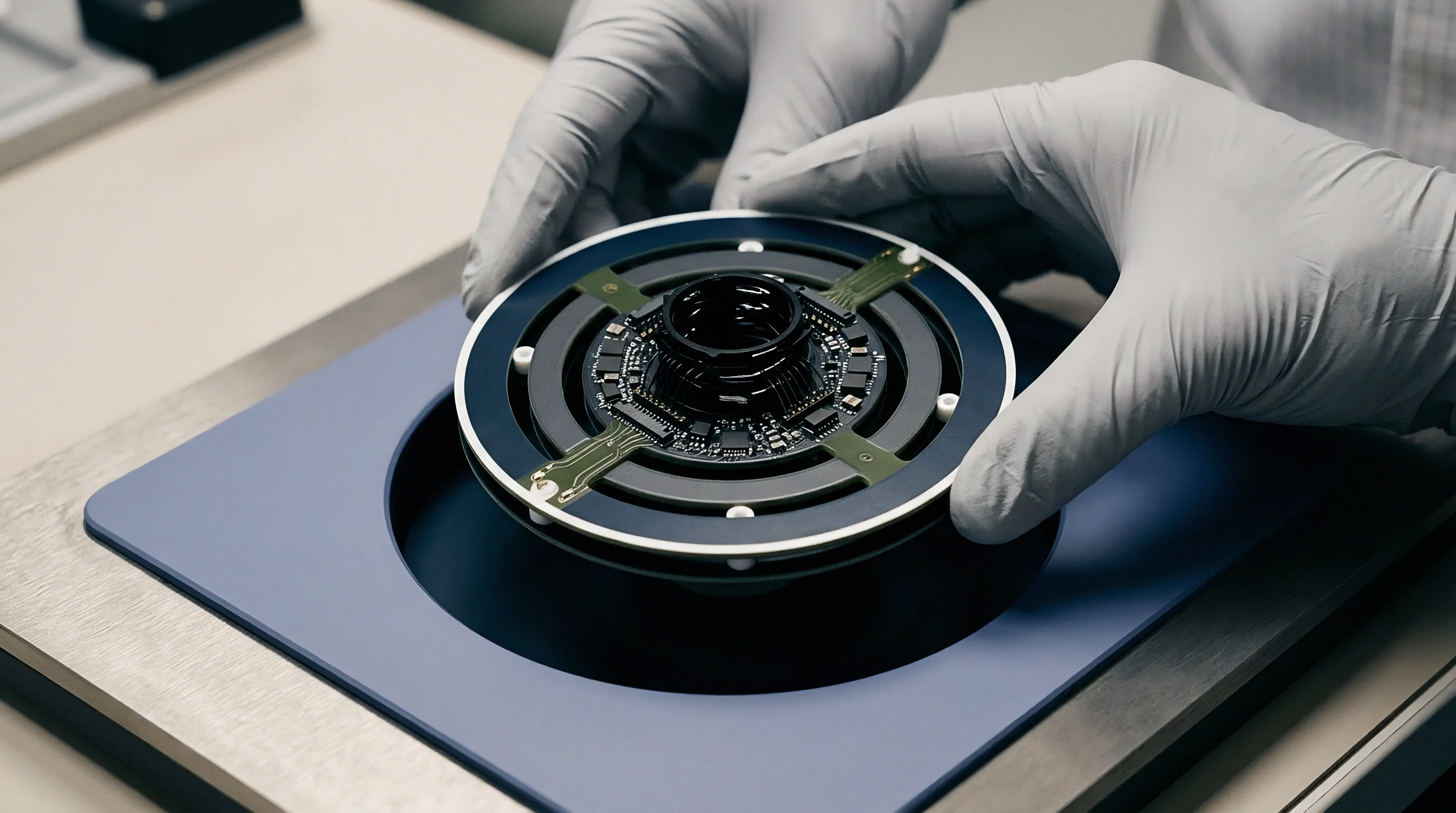
Procuring non-volatile memory for high-temperature industrial equipment demands careful commercial and engineering auditing. Silicon vendors price chips based on thermal qualification grade, array density, process node maturity, and guaranteed retention lifespan. Commercial flash chips certified up to 85°C fail quickly in harsh industrial settings due to thermal discharge and data corruption.
Automotive qualification standards define benchmarks for high-temperature silicon. AEC-Q100 Grade 1 specifies operation from -40°C to +125°C ambient, while AEC-Q100 Grade 0 extends requirements from -40°C to +150°C. Genuine Grade 0 certified flash memory carries a substantial price premium over commercial parts due to extensive vendor burn-in testing, lower wafer yields, and specialized ceramic packaging.
Retention guarantees are a frequent source of dispute between integrators and silicon vendors. Datasheets often quote ten-year retention, but fine print restricts that figure to a 25°C average operating temperature ~ at 150°C, guaranteed retention drops to weeks or days. Sourcing contracts must explicitly define retention expectations at actual operating temperatures, including remedies and lot replacement terms for early failures.
Wafer Fabrication Temperature Grading Costs
Fabricating high-temperature silicon requires specialized process steps that drive up wafer production costs. Commercial flash relies on thin gate oxides and dense cell layouts optimized for room temperature. Grade 0 memory uses thicker gate dielectrics, specialized nitridation, and longer channels to resist thermal tunneling, which reduces bit density per square millimeter of silicon.
Wafer screening and burn-in testing add substantial cost to Grade 0 parts. Fabs run high-temperature stress screening (HTSS) and extended bakes to weed out dies with latent micro-defects. This screening reduces usable die yields per wafer by 15% to 35%, driving up unit pricing for certified parts.
Commercial Warranty Terms and Retention Guarantees
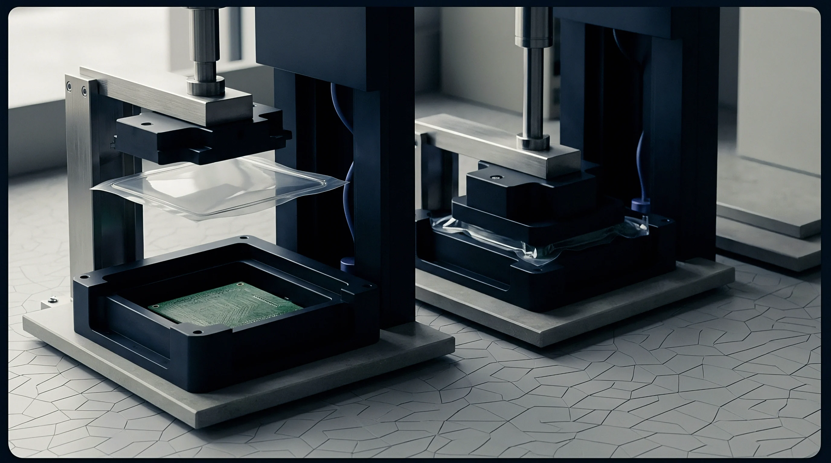
Standard IC purchase agreements disclaim liability for data corruption near upper thermal limits. Vendors often contest warranty claims by arguing that system thermal management allowed junction temperatures to exceed maximum ratings during plant operational spikes. Sourcing teams must demand explicit contractual language defining retention performance under continuous worst-case thermal stress.
Procurement contracts should require full qualification dossiers from suppliers, including raw multi-temperature bake data, extracted activation energy spectra, and tail-cell distribution metrics. Certificates of compliance leave buyers vulnerable to unannounced process changes that degrade high-temperature retention. Clauses ought to tie lot payment releases directly to independent third-party lab verification of storage life metrics.
- Multi-Temperature Retention Dossier The supplier must provide raw threshold voltage distribution decay curves from 150°C, 175°C, and 200°C stress bakes.
- Activation Energy Derivation Sheet Sourcing documentation must show empirical extraction of activation energies across the operational temperature spectrum.
- Tail-Cell Distribution Metrics Qualification records must report retention statistics for the worst-performing 0.001% of array cells rather than median values.
- Process Change Notification Agreement Contracts must require formal notification and re-qualification approval prior to any fab process alteration.
Yields fall under thermal testing, driving up sourcing costs. Procurement teams should verify thermal test dossiers before committing to component volumes. Inspecting retrieved transceiver boards reveals oxide stress lines concentrated near high-power RF power amplifiers where local junction temperatures exceed ambient ratings.
| Thermal Grade | Operating Range (°C) | Relative Unit Price Multiplier | Wafer Test Yield Fallout | Guaranteed Retention at 150°C (Unrefreshed) |
|---|---|---|---|---|
| Commercial | 0 to +70 | 1.0× | Unspecified (Fails | |
| Industrial | -40 to +85 | 1.35× | 3% to 5% | 7 days |
| Automotive Grade 1 | -40 to +125 | 2.10× | 8% to 12% | 90 days |
| Automotive Grade 0 | -40 to +150 | 4.50× | 18% to 35% | 5 years (with rated ECC) |
Section 8.2 of industrial supply contract document ELEC-QUAL-2024 mandates that silicon suppliers assume full warranty replacement liability for assembled radio modules if lot retention screening fails to demonstrate five-year data survival under continuous 140°C thermal exposure.