Meaning
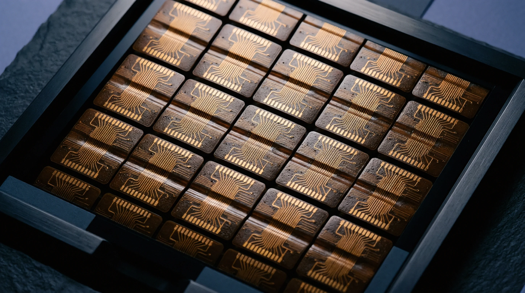
Production losses measured as the number of defective dies on a silicon wafer indicate the efficiency of the semiconductor fabrication process. Engineers track wafer yield fallout to identify systematic errors in the lithography or etching stages. High rates of loss increase the unit cost of the remaining functional parts.
Process Variance
Small changes in the cleanroom environment or the chemical concentration can lead to clusters of failures. Analyzing the patterns of wafer yield fallout helps technicians find the specific machine that is out of calibration. If the defects are concentrated at the edge of the wafer, it might suggest an issue with the uniformity of the plasma deposition.
Economic Impact
Profitability in the chip industry depends on keeping the number of good dies per wafer as high as possible. Wafer yield fallout is the primary factor that determines the break even point for a new manufacturing node. A company might lose millions of dollars if a specific batch of wafers shows an unexpected spike in defects.
Defect Analysis
Automated inspection tools scan the surface of every wafer to map the location of every failed circuit. This data on wafer yield fallout is fed back into the design software to improve the layout of future products. By making the circuit patterns less sensitive to small particles, designers can reduce the fallout and increase the total output of the factory.
This continuous improvement cycle is what allows for the steady reduction in the price of memory and processors.