Sub-GHz Transceiver Crystal Passivation under Extended High Current Transmit Pulses
Sub-GHz transceiver crystal passivation prevents drive-level dependency shifts and frequency pulling during extended high-current power amplifier transmit pulses.

Stress
Sub-GHz transceivers in smart utility meters, industrial telemetry, and wide-area monitoring send long data pulses at high output power levels. A power amplifier drawing up to 500 mA at +30 dBm output creates sharp thermal gradients inside the module enclosure. Heat from the power silicon travels through copper ground pours directly into adjacent crystal resonator packages.
This temperature differential puts mechanical strain on the quartz crystal blank, pulling its fundamental resonant frequency off target during the transmit burst.
Energy delivered over multi-second transmissions alters crystal behavior far beyond simple static temperature drift. Differential thermal expansion creates shear forces at the boundary between the quartz blank and its metal electrodes. Gold or silver metallization layers expand at rates vastly different from single-crystal quartz.
Under repeated long transmit bursts, these interfacial stresses drive defect migration and micro-fissuring near electrode margins.

Thermal Dissipation Dynamics in High Power Bursts
Heat transfer inside a compact Sub-GHz system-on-module happens quickly through shared ground planes. During a three-second continuous FSK pulse at 915 MHz with +27 dBm output, power amplifier junction temperatures jump by more than 40 degrees Celsius. Inner copper layers carry this heat spike to the crystal solder pads in milliseconds, subjecting the crystal package to asymmetric thermal flux that heats one end of the resonator before the other can equalize.
Temperature imbalances across the quartz plate trigger transient frequency shifts that integrated temperature compensation logic cannot catch. Thermistor sensors embedded in modern transceiver chipsets only sample ambient package temperatures periodically, missing the fast local temperature spikes right inside the crystal enclosure. As a result, carrier frequency offset spikes during the first half of an extended transmit pulse, causing packet reception failures at remote gateway nodes.
| Transmit Power (dBm) | Pulse Duration (ms) | PA Current (mA) | Crystal Package Temp Rise (°C) | Peak Carrier Offset (ppm) |
|---|---|---|---|---|
| +14 | 100 | 45 | 0.2 | 0.4 |
| +20 | 500 | 120 | 1.8 | 1.9 |
| +27 | 2000 | 340 | 6.5 | 7.2 |
| +30 | 5000 | 520 | 14.1 | 16.8 |
Quartz Resonator Mechanical Overdrive
High RF output power demands strong drive signals from the transceiver phase-locked loop oscillator core. When internal driver circuits increase current to sustain oscillation under heavy loads, mechanical drive levels in the crystal blank rise alongside it. Quartz mechanical displacement scales directly with applied AC voltage across its electrodes, so high drive levels induce substantial shear strains inside the vibrating crystal lattice.
Excessive displacement amplitudes force the quartz lattice into non-linear elastic regimes. This distorts the harmonic purity of the oscillation reference, generating phase noise sidebands across adjacent Sub-GHz channels. Over long pulse profiles, non-linear mechanical excitation accelerates atomic movement along crystallographic fault lines, turning small material imperfections into physical dislocations that permanently shift frequency calibration.
Mechanical fatigue accumulates inside the quartz over millions of transmit cycles. High current pulses act like physical hammers striking the quartz plate at its resonant frequency. Peak shear force lands around the perimeter of the crystal blank, where epoxy mounts secure the plate to the ceramic package base.
Microscopic delamination at these mounting points increases equivalent series resistance, cutting into oscillator loop margin.
Good layout isolation buffers the quartz package from severe thermal shocks. Placing thermal relief cutouts around crystal solder pads slows heat transfer from internal ground planes, while orienting the crystal package axis perpendicular to the power amplifier’s main heat dissipation vector balances temperature gradients across both electrode leads. Careful physical layout keeps local thermal surges away from the resonator core.
Sustained thermal exposure speeds up internal chemical reactions inside sealed crystal packages. Residual moisture trapped during manufacturing reacts with metallic electrodes under elevated electro-mechanical drive. Oxidation layers form along silver or aluminum electrode surfaces, changing the physical mass of the vibrating assembly and pulling the fundamental resonant frequency downward over its operating life.
Thermal gradients also destabilize internal gas pressures inside hermetically sealed seam-welded packages. Traces of noble gas or nitrogen in the cavity undergo localized pressure expansion during rapid heating pulses, exerting fluid forces against the thin quartz plate surface. This extra mechanical loading worsens frequency instability during maximum-power bursts.
Maintaining thermal stability comes down to balancing PCB ground plane copper weight against the module’s thermal dissipation pathways.
Layer
Surface passivation layers on quartz crystal resonators protect bare quartz blanks and metallic electrodes from environmental degradation. Atomic layer deposition and vacuum thin-film evaporation deposit ultrathin dielectric barriers ~ such as aluminum oxide or silicon dioxide ~ directly over quartz plate surfaces. These barriers prevent chemical reactions between ambient package gases and active metal electrodes, which would otherwise allow high current pulses to drive volatile contaminants onto active vibrating areas.
Thin chemical coatings shield crystal surfaces against outgassing from internal structural adhesives. Conductive epoxies used to mount quartz blanks on ceramic substrates contain organic polymers that release volatile organic vapors into the sealed cavity when warmed by high-power transmit pulses. The passivation layer forms a dense barrier that keeps hydrocarbon molecules from condensing onto the active quartz channel.
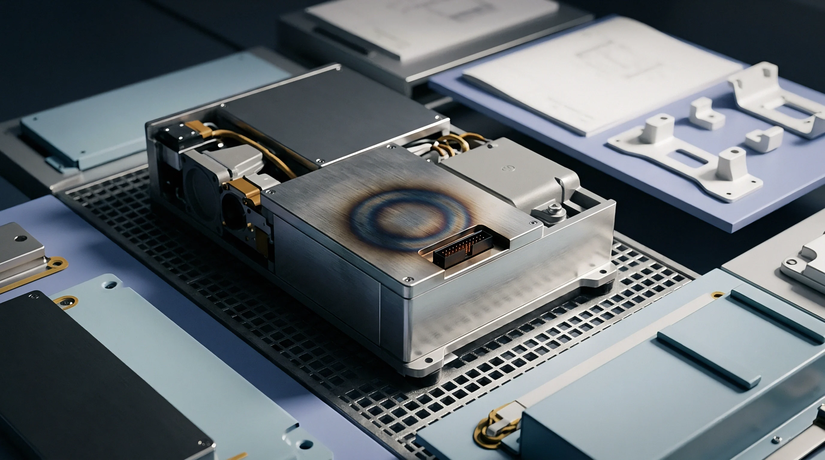
Atomic Layer Deposition for Electrode Protection
Atomic layer deposition coats quartz crystal blanks with pinhole-free dielectric films down to atomic scale precision. Alternating gas-phase precursor reactions build uniform aluminum oxide matrix layers over irregular electrode edges. This dense atomic structure blocks ionic migration along quartz surfaces during high current pulses, maintaining elasticity while sealing microscopic surface fractures on raw quartz plates.
Bare metal electrodes oxidize when exposed to trace oxygen during extended high power pulses. Passivation layers seal electrode surfaces, preventing chemical transformations that alter crystal mass. Aluminum oxide layers under twenty nanometers thick preserve quartz quality factors without adding unwanted mechanical damping, keeping equivalent series resistance steady while blocking chemical decay.
Gold electrode surfaces coated with a fifteen-nanometer alumina passivation film show zero frequency drift under twenty-thousand hours of continuous pulsed RF stress at eighty-five degrees Celsius.

Outgassing Species under Intermittent Thermal Pulses
High current transmit pulses trigger rapid thermal cycling that speeds up outgassing inside package voids. Polymer epoxies release volatile siloxanes, moisture, and unreacted monomer residues as temperatures climb during high-power bursts. Free molecules move across the cavity, drawn by electrostatic fields around the vibrating quartz electrodes, where condensation adds mass and causes sudden frequency shifts.
Passivation lowers surface energy on quartz plates, keeping organic vapors from sticking to critical vibration zones. Non-passivated blanks attract organic molecules that form sticky films under continuous RF drive. These hydrocarbon layers absorb mechanical energy from the vibrating quartz, sharply increasing internal friction and degrading the crystal quality factor until transceiver phase-locked loop synthesizers go unstable.
Testing evaluated three distinct crystal encapsulation technologies under extended high current transmit burst profiles. Modern surface-mount crystals rely on glass-frit sealed ceramic packages, seam-welded metal lid enclosures, or resin-molded packages. Seam-welded metal enclosures using ultra-clean gold-tin preform seals exhibited the lowest levels of internal cavity contamination under pulsed drive testing.
- Hydrocarbon Condensation Vapors outgassed from structural epoxies settle on non-passivated electrodes during cooling cycles, permanently shifting resonant frequency downward.
- Ionic Surface Migration Trace alkali ions move across unpassivated quartz surfaces under strong electric fields, causing localized current leakage and frequency drift.
- Electrode Oxidation Reactive oxygen species corrode silver alloy electrodes under high thermal drive, increasing equivalent series resistance over extended transmit lifetimes.
- Dielectric Film Cracking Brittle passivation layers fracture under high amplitude mechanical displacement, exposing bare underlying quartz lattice to chemical decay.
Cracks in passivation layers create pathways for chemical attack along quartz crystal boundaries. Continuous mechanical flexing from high drive levels subjects passivation coatings to cyclic strain. Materials chosen for passivation layers must match the thermal expansion coefficient of the underlying quartz blank; an expansion mismatch induces micro-cracking across passivation surfaces during temperature swings.
The chemical stability of the passivation layer dictates crystal lifespan in demanding sub-GHz smart grid applications. Silicon dioxide offers excellent mechanical lattice matching on quartz blanks, but provides a weaker moisture barrier than aluminum oxide. Hybrid multi-layer stacks that alternate silica and alumina combine high mechanical flexibility with low chemical permeability under intense pulse stress.
Manufacturing cleanrooms must strictly control organic contamination during passivation processing. Trace airborne contaminants trapped beneath passivation layers create localized defects during high current transmit bursts. Surface preparation steps ~ including plasma cleaning and vacuum bakeouts ~ strip organic residues before thin-film deposition, ensuring long-term adhesion of protective coatings.
Standard commercial quartz packages undergo outgassing burn-in during assembly, but high-power Sub-GHz applications still require secondary passivation.


Excitation
Continuous RF transmit pulses require high oscillator drive current to sustain phase stability across wide temperature ranges. Transceiver phase-locked loops feed high voltage swing waveforms into crystal driver pins to lower phase noise during modulation. High drive levels increase piezoelectric displacement within quartz blanks, forcing mechanical vibrations past linear boundaries.
Overdriving quartz crystal resonators leads to severe parameter degradation, including drive level dependency shifts and spurious frequency jumps.
Oscillator design balance dictates long-term frequency stability under maximum RF power burst conditions. Designing crystal driver circuits with excessive loop gain guarantees fast startup times, but subjects quartz blanks to mechanical overdrive. Excess drive power converts directly into heat inside the quartz plate, aggravating thermal gradients.
Circuit design has to balance fast start-up constraints against long-term quartz lattice protection.
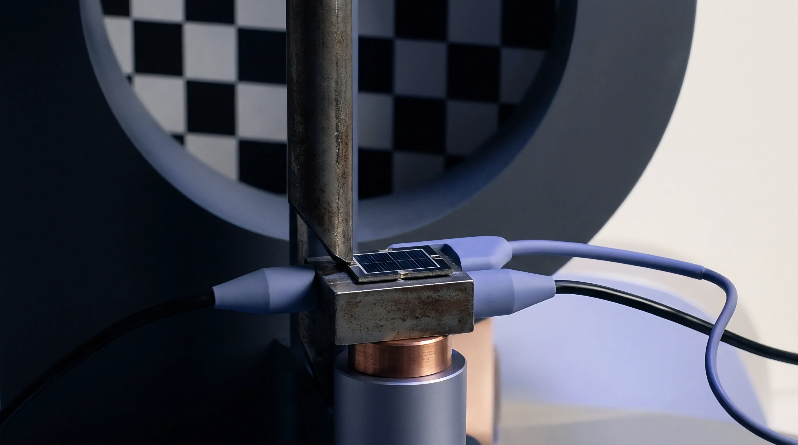
What Overdrive Level Triggers Dynamic Lattice Dislocation?
Drive levels exceeding two hundred microwatts introduce non-linear stress waves into standard miniature surface-mount quartz crystal blanks. At these power levels, mechanical shear strains exceed internal atomic binding thresholds along quartz crystallographic axes. Slippage between crystal lattice planes causes permanent structural dislocations, creating microscopic defect pockets in the quartz volume that manifest as irreversible frequency offsets remaining after cooling.
Severe overdrive causes activity dips where crystal frequency and equivalent series resistance shift rapidly over narrow temperature ranges. These dips occur when fundamental mode vibration couples mechanically with unwanted high-order overtone or flexural modes. Structural dislocations induced by high drive current lower the energy threshold for mode coupling, causing transceivers that hit an activity dip during transmission to instantly lose phase lock and terminate radio links mid-packet.
Drive levels above one hundred microwatts applied to small footprint sub-GHz crystals double the rate of permanent frequency aging compared to lower power excitation regimes.

Equivalent Series Resistance Shift Metrics
Equivalent series resistance reflects total electrical loss inside a vibrating crystal package assembly. High current transmit pulses cause micro-friction between quartz blanks, metallic electrodes, and internal structural adhesives. This friction degrades equivalent series resistance, forcing transceiver crystal oscillator circuits to draw extra current to sustain oscillation.
When resistance rises past internal oscillator gain limits, oscillation fails completely.
| Modulation Standard | Frequency Band (MHz) | Applied Drive Level (µW) | Baseline ESR (Ω) | Post-Stress ESR (Ω) | Frequency Aging (ppm) |
|---|---|---|---|---|---|
| 2-GFSK (100 kbps) | 868.3 | 50 | 22.4 | 23.1 | +0.8 |
| Wireless M-Bus N mode | 169.4 | 100 | 18.9 | 20.5 | +1.4 |
| IEEE 802.15.4g SUN | 915.0 | 250 | 21.0 | 28.7 | +4.2 |
| LoRaWAN (SF12 / 125 kHz) | 923.0 | 500 | 19.5 | 37.2 | +9.6 |
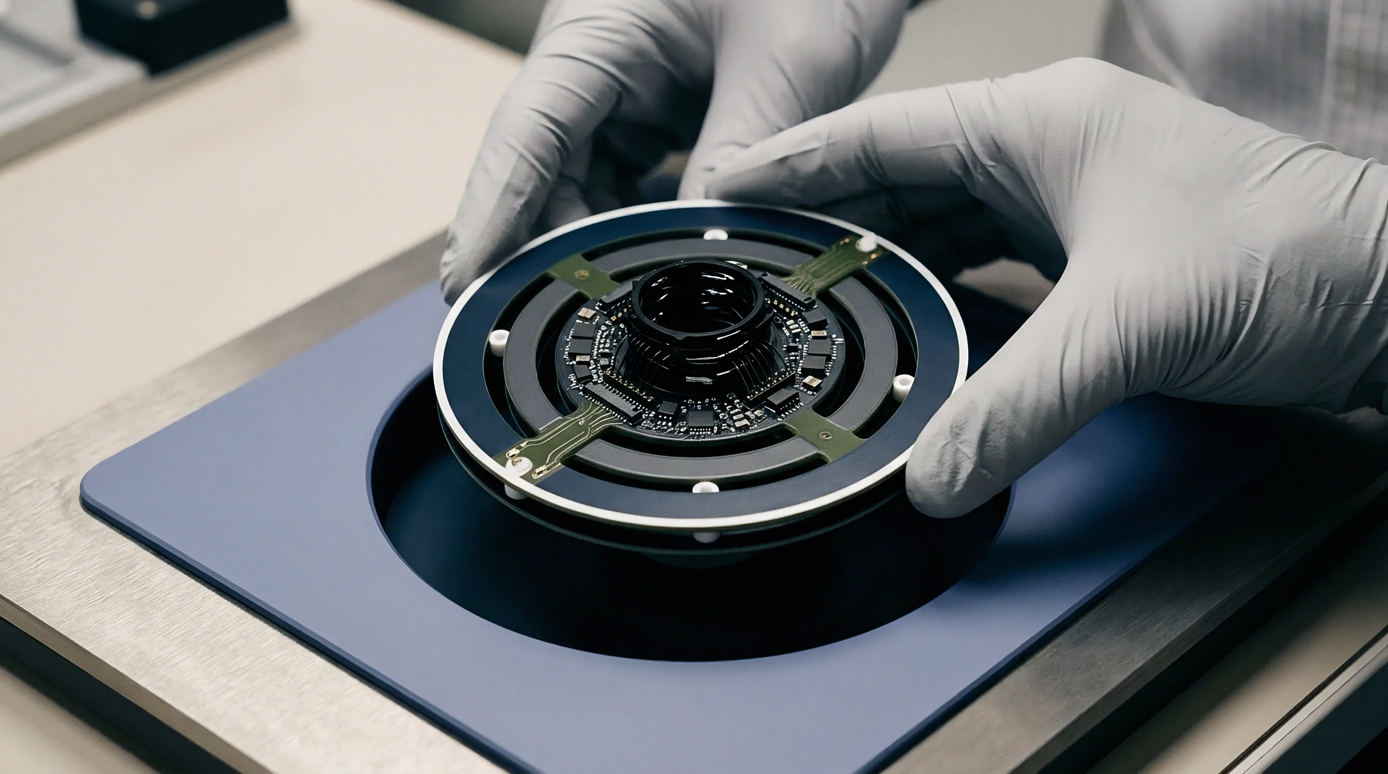
Frequency Pulling under Power Amplifier Current Spikes
Power amplifier stages drawing large current pulses depress local supply voltages on transceiver silicon dies. Voltage droop along supply traces alters oscillator inverter stage capacitance, pulling crystal load capacitance off baseline. These load capacitance shifts cause instant carrier frequency pulling as transmit bursts ramp up, distorting output spectra and driving adjacent channel power ratio violations during compliance testing.
Decoupling capacitor selection and physical placement mitigate voltage droop on transceiver crystal oscillator pins. Low equivalent series inductance ceramic capacitors placed right next to oscillator power supply pins deliver quick charge during high-power transmit transitions. Isolating oscillator power rails with ferrite beads keeps high-frequency switching regulator noise out of crystal driver circuits.
A drive-level dependency test sequence maps parameter drift against excitation power levels.
- Mount crystal samples inside temperature-controlled RF test fixtures maintained at twenty-five degrees Celsius.
- Connect an RF network analyzer to measure baseline series resonant frequency and equivalent series resistance at a low drive level of one microwatt.
- Increase drive level incrementally from one microwatt to five hundred microwatts in ten logarithmic steps, holding each power step for sixty seconds.
- Record frequency and equivalent series resistance values at every power step to build drive level dependency characteristic curves.
- Return drive level back to one microwatt and record post-stress baseline values after a fifteen-minute stabilization period.
- Calculate permanent drive level dependency frequency shift and equivalent series resistance change percentages.
Continuous operation at elevated drive power accelerates fundamental aging in piezoelectric quartz. Surface contamination moves rapidly when high drive voltages create strong electrostatic gradients across electrode gaps. Ionic species within package gases drift toward electrode edges over time, building conductive bridges that degrade quality factors and elevate phase noise.
Harmonic distortion from overdriven crystal resonators degrades receiver performance in half-duplex transceiver systems. Spurious harmonics generated during transmit pulses linger as mechanical vibrations during immediate transmit-to-receive transitions. This lingering ringing feeds spurious signals back into transceiver low-noise amplifiers, degrading sensitivity during rapid-response acknowledge windows.
Piezoelectric stress distribution across custom crystal blank geometries dictates maximum allowable drive levels. AT-cut quartz plates shaped with contoured or beveled edges concentrate vibration energy into the center of the blank, away from package mounts. This energy trapping cuts mounting losses, lowering baseline equivalent series resistance while increasing tolerance against high current drive bursts.
Oscillator loop gain margins must accommodate crystal equivalent series resistance growth over a product’s operating lifetime. Designing oscillator circuits with at least a five-times gain margin ensures reliable startup under worst-case resistance growth; insufficient margin leads to intermittent start-up failures in field devices deployed in cold environments after years of pulse stress.
Ignoring quartz drive level limits leads to sudden, field-wide radio transceiver failures that invalidate operational battery life models and corrupt network synchronization timing.


Screening
Comprehensive screening protocols verify passivated crystal resonator integrity before integration into high-reliability Sub-GHz modules. Standard commercial quality testing fails to catch latent drive level dependency defects or weak passivation layers. Specialized test programs apply continuous pulsed RF drive, thermal shock cycling, and acoustic emission monitoring to screen out marginal components and prevent costly field failures.
Production screening isolates crystal batches prone to premature aging or activity dips under high power transmit profiles. Screening test suites evaluate parameter stability before and after high drive pulse stress. Automated test equipment measures frequency shift, equivalent series resistance growth, and phase noise degradation across operating temperature limits, generating data that directly guides vendor selection and quality audits.

Accelerated Life Testing under Continuous Pulsed Drive
Accelerated life testing subjects crystal samples to thousands of simulated high current transmit pulses at elevated temperatures. Test chambers hold ambient temperature at eighty-five degrees Celsius while high power drive signals stress internal quartz resonators continuously for one thousand hours, with regular parameter measurements mapping decay trajectories over simulated ten-year lifespans.
Pulsed-drive accelerated testing reveals contamination outgassing and passivation breakdown mechanisms faster than static burn-in. Rapid thermal expansion cycles induce mechanical stresses that crack defective passivation films; crystals that survive demonstrate stable frequency retention and low equivalent series resistance growth in the field.
| Test Standard | Parameter Assessed | Test Conditions | Pass / Fail Threshold |
|---|---|---|---|
| AEC-Q200-009 | Drive Level Dependency | 1 µW to 500 µW sweep | ESR change < 10% |
| MIL-STD-883 M1014 | Hermetic Seal Integrity | Fine/gross leak helium detection | Leak rate < 5×10^-8 atm cc/s |
| JESD22-A104 | Thermal Temperature Cycling | -40°C to +105°C, 1000 cycles | Frequency drift < 5 ppm |
| Internal Pulse Spec | High Drive Pulse Endurance | +27 dBm TX pulses, 50% duty, 500 hrs | Zero activity dips observed |
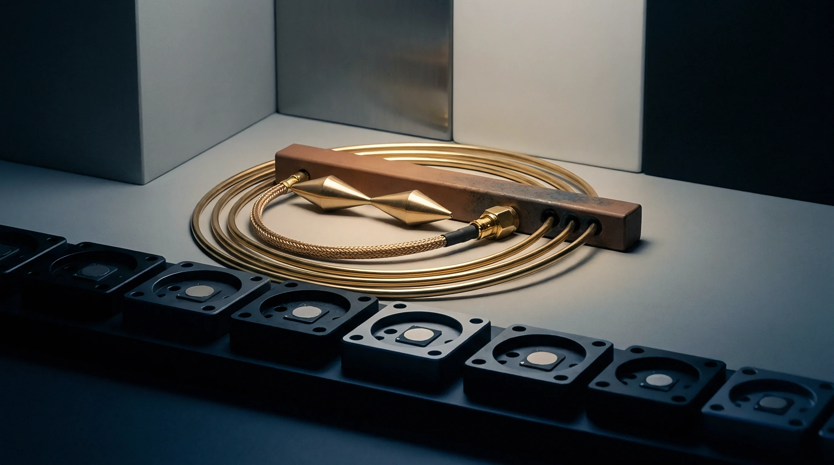
Acoustic Emission Monitoring for Microcrack Detection
Acoustic emission monitoring detects microscopic structural failures inside quartz crystal blanks during high drive pulse testing. Ultra-sensitive piezoelectric transducers attached to ceramic packages capture high-frequency acoustic stress waves emitted when lattice microcracks propagate, catching physical damage long before electrical parameter shifts show up on RF spectrum analyzers.
Microcracking sound signatures show distinct energy spikes in the megahertz frequency spectrum. Filtering background mechanical noise lets automated test stations isolate cracking events during pulse application, rejecting units before fragile components reach assembly lines.
Contractual sourcing terms dictate that crystal batches exhibiting greater than two percent failure rates during drive level dependency screening undergo full lot rejection at supplier expense.
Screening decision guidelines help hardware qualification teams select suitable crystal components for long-pulse Sub-GHz designs.
- Verify Hermetic Seal Ratings Select crystal packages verified by helium mass spectrometer leak detection to guarantee low cavity contamination rates.
- Audit Passivation Layer Uniformity Demand transmission electron microscopy cross-section data from suppliers to verify consistent passivation thickness over electrode edges.
- Evaluate Drive Level Dependency Curves Reject crystal designs showing equivalent series resistance increases exceeding fifteen percent between low and high drive test points.
- Screen for Temperature Activity Dips Run high-resolution frequency sweeps across the full operating temperature spectrum to detect localized mode coupling points.
Lot acceptance testing must incorporate dynamic drive pulse stress steps prior to final parameter sign-off. Measuring crystal parameters only under static room temperature conditions hides internal defects that trigger failures under actual transmit pulse stress. Pulsed screening protocols simulate real transceiver operation to secure overall module reliability.
Screening protocols must explicitly mandate drive level dependency verification across full temperature ranges per standard compliance annexes.
Dossier
Technical sourcing dossiers define mandatory crystal passivation, packaging, and screening requirements for high-power Sub-GHz module procurement. Sourcing documents translate physical reliability requirements into enforceable legal and engineering specifications for component suppliers, covering quartz material quality, electrode passivation chemistries, hermetic sealing methods, and lot acceptance parameters to protect module buyers against unannounced vendor material changes.
Procurement dossiers establish technical baselines that protect teams during quality disputes over field failures. Standard commercial crystal datasheets lack detailed specifications covering drive level dependency limits, outgassing thresholds, or passivation film compositions. Detailed procurement specifications mandate precise manufacturing processes, forcing crystal vendors to tightly control sub-tier material supply chains.

Specification Clauses for Crystal Package Hermeticity
Package hermeticity clauses define strict allowable leak rates for crystal voids to prevent moisture ingress over fifteen-year product lifespans. Specifications mandate fine helium leak testing under MIL-STD-883 standards alongside gross leak fluid immersion checks, limiting water vapor inside package cavities to less than five hundred parts per million at room temperature.
Sealing glass chemistry specifications prohibit volatile additives that outgas during seam-welding or glass-frit processing. Sourcing contracts require manufacturers to use low-outgassing gold-tin alloy preforms or inorganic glass seals. Controlling internal package chemistry eliminates organic contamination sources that compromise passivation layers under high current pulse drive.
Single-source procurement strategies for sub-GHz reference crystals expose module manufacturers to unmitigated field recall liabilities when vendor process changes alter passivation film integrity.

Batch Verification and Receiving Inspection Audit
Receiving inspection audits enforce batch compliance by testing incoming crystal lots against dossier parameters prior to production release. Quality assurance protocols pull random samples from each shipment for destructive physical analysis and drive level dependency testing, while traceability rules mandate lot-specific certificates of analysis detailing electrode passivation thickness.
Plant audits verify that crystal suppliers maintain cleanroom environmental controls during blank processing and passivation. Inspection protocols evaluate vendor cleanroom air filtration, wafer washing water purity, and operator handling procedures. Regular supplier audits prevent cleanroom contamination drift from compromising crystal passivation quality.
| Dossier Requirement Clause | Target Specification | Verification Method | Commercial Consequence of Non-Compliance |
|---|---|---|---|
| Passivation Layer Thickness | 15 nm ± 2 nm Al2O3 | Ellipsometry / TEM Cross-section | Immediate batch return at supplier cost |
| Drive Level Dependency | < 10% ESR shift up to 300 µW | Automated drive sweep test | Lot rejection and re-qualification penalty |
| Package Internal Moisture | < 500 ppm H2O volume | Residual Gas Analysis (RGA) | Supplier payment hold pending audit |
| High Current Aging Rate | < 2 ppm shift over 1000 hrs TX | Accelerated life test chamber | Warranty liability clause enforcement |
Supply chain documentation must require written notification twelve months prior to any proposed change in crystal passivation materials, processing equipment, or manufacturing locations. Unannounced supplier changes in electrode metallization or passivation deposition parameters regularly introduce latent field reliability defects. Contractual change control clauses give module integrators sufficient time to perform full re-qualification testing before modified components enter production.
Module pricing calculations must account for the added cost of high-grade passivated quartz crystals versus standard commercial resonators. Premium seam-welded crystals with atomic layer passivated electrodes cost significantly more than standard components. Skipping them lowers initial BOM costs, but exposes the design to field failure rates that dwarf those initial component savings.
Documenting second-source qualification pathways inside the technical dossier prevents production line halts caused by primary supplier shortages. Secondary crystal suppliers must pass the identical suite of high current drive pulse, thermal shock, and passivation integrity screening protocols. Maintaining two qualified, audited crystal suppliers ensures continuous manufacturing capability without sacrificing field reliability.
Which chemical passivation stack optimized for sub-GHz crystal electrodes guarantees zero frequency drift under twenty-dBm transmit bursts across extended operational lifespans?