SubGHz High Power Switch Passivation Stack Selection Basics
Sub-GHz high-power switch passivation requires a low-defect oxide interface beneath dense silicon nitride buffered by polyimide to stop RF field trapping.


Stress
Sub-gigahertz transmitters operating between 169 MHz and 915 MHz routinely push terminal power to +30 dBm in smart utility meters and up to +37 dBm in rural fixed-wireless access points. Placed directly after the power amplifier, a transmit switch faces continuous peak-to-peak radio-frequency swings above 65 volts under severe load mismatch. Dielectric layers over the active periphery carry that full electric field gradient across sub-micron channel boundaries.
In silicon-on-insulator switch field-effect transistors and gallium nitride high-electron-mobility transistors, failure occurs when these localized peak fields inject electrons into unpassivated interface states or puncture thin inter-electrode insulator films.
Passivation stacks govern both the maximum RF voltage swing and long-term insertion loss stability at these high-power switch nodes. Under alternating fields cycling hundreds of millions of times per second, carriers get driven into defect traps at the dielectric-semiconductor boundary. That trapped charge shifts channel surface potential and generates third-order harmonic distortion products.
An inadequate stack permits gradual threshold voltage drift during active transmission, degrading insertion loss by fractions of a decibel over a fifteen-year design life.
A transmission mismatch of ten-to-one voltage standing wave ratio elevates switch node peak swings beyond sixty-five volts under one-watt carrier drives.
Stack selection forces a trade-off between breakdown field strength, parasitic substrate capacitance, and mechanical film stress. Silicon nitride from plasma-enhanced chemical vapor deposition gives high breakdown strength and moisture resistance, but a relative dielectric constant of 7.0 adds parasitic capacitive loading. Thick spin-on polyimide or benzocyclobutene coatings cut capacitance via relative dielectric constants below 2.8, but cannot stop moisture ingress without an inorganic barrier underneath.
RF front-end module designers therefore pair thin inorganic films with stress-relieving organic overcoats to build stacks that survive continuous high-power radio-frequency exposure.
Dielectric
Inorganic thin films provide the primary seal over switch gate electrodes and source-drain ohmic contacts. High-power Sub-GHz switch architectures rely on these first few nanometers of dielectric to satisfy surface dangling bonds and suppress gate-edge leakage. Plasma-deposited silicon dioxide forms at moderate temperatures with low interface state densities against silicon, and an 8 megavolt per centimeter breakdown field handles sharp peak voltage swings.
However, porous film microstructure allows gradual moisture permeation, eventually degrading switch isolation in humid environments.
Silicon nitride remains the standard diffusion barrier across radio-frequency silicon-on-insulator and compound semiconductor switch processes. Adjusting the silane-to-ammonia gas ratio tunes film stoichiometry, swinging internal stress from tensile to compressive. Silicon-rich formulations yield refractive indexes above 2.05 with higher electrical conductivity, dissipating RF energy into the dielectric and hurting switch harmonic suppression.
By contrast, stoichiometric, nitrogen-rich nitride deposited at 300 degrees Celsius maintains loss tangents below 0.001 at 900 MHz while blocking sodium ions and water molecules entirely.
Atomic layer deposition of aluminum oxide offers conformal step coverage over sharp gate topography where plasma-assisted methods fall short. With a relative dielectric constant near 9.0 and breakdown fields reaching 9 megavolts per centimeter, ALD alumina forms a pinhole-free base across high-aspect switch geometries. Controlling film stress is critical, however, as excessive tensile stress leads to microcracking during packaging reflow.
| Material Formulation | Deposition Method | Dielectric Constant | Breakdown Field (MV/cm) | Loss Tangent (900 MHz) | Internal Stress (MPa) |
|---|---|---|---|---|---|
| Silicon Dioxide (SiO2) | PECVD (350 deg C) | 3.9 | 8.0 | 0.0008 | -150 Compressive |
| Stoichiometric Nitride (Si3N4) | PECVD (300 deg C) | 7.0 | 9.5 | 0.0012 | +250 Tensile |
| Silicon-Rich Nitride (SiNx) | PECVD (250 deg C) | 7.6 | 6.5 | 0.0065 | -300 Compressive |
| Aluminum Oxide (Al2O3) | Thermal ALD (250 deg C) | 9.1 | 9.0 | 0.0020 | +350 Tensile |
| Benzocyclobutene (BCB) | Spin Coat (250 deg C cure) | 2.65 | 3.5 | 0.0008 | +30 Tensile |
| Photosensitive Polyimide | Spin Coat (320 deg C cure) | 3.2 | 4.0 | 0.0025 | +45 Tensile |
Polymer buffers sit atop the stack to shield diced die from packaging stresses. During thermal cycling between -40 and +105 degrees Celsius, plastic mold resins exert localized shear exceeding 80 megapascals. Without a three- to five-micrometer polyimide buffer, this lateral force couples straight into brittle underlying nitride, driving delamination along metallization edges.
Cure schedules for spin-on polyimide must also stay within thermal limits set by back-end copper interconnects to avoid copper voiding.

Drift
Passivation layers on high-power switch dies rarely stay inert under load. Large alternating voltage swings drive channel carriers into deep-level traps at the dielectric-semiconductor interface. In Sub-GHz bands, carrier transit across the channel takes fractions of a picosecond, yet trap emission spans milliseconds to full seconds.
This disparity causes steady surface charge accumulation that shifts the effective threshold voltage across outer switch branches.
That drift shows up electrically as power-dependent insertion loss growth. Sustained transmission at +33 dBm builds up charge that pulls off-state switch branches toward partial inversion. These inactive branches start leaking RF current to ground, generating heat and degrading link margins.
Higher junction temperatures worsen the effect by thermally activating deeper trap states within the dielectric bandgap.
Trapping lifetimes exceeding the carrier period create permanent DC polarization shifts across high-voltage RF switch terminals.
Passivation choices dictate how the switch responds to strong transmitter phase mismatch conditions.
- Gate fringe field concentration drives rapid carrier injection into lower-density dielectric directly above the drain drift zone.
- Porous oxide moisture retention supplies hydroxyl ions that raise the dielectric loss tangent over field deployment.
- Nitride charge trapping builds localized sheet charge that skews reverse-bias channel pinch-off behavior.
- Polymer cure shrinkage induces compressive strain that shifts piezoelectric coefficients in compound semiconductor substrates.
Mitigating these charge effects requires an engineered interface. Depositing an ultra-thin silicon dioxide interlayer before bulk silicon nitride passivates dangling silicon bonds, suppressing surface trap density below 10 to the 10th power per square centimeter electron-volt. Omitting this step allows surface states to multiply, degrading channel power handling and forcing transmitter switch derating.

Foil
Passivation stack stress dictates whether an assembly survives thermal shock testing. High-power Sub-GHz modules assemble bare switch die alongside matching networks on laminate carriers under silica-filled epoxy encapsulants. Differences in thermal expansion induce sharp bending moments across the thinned die: silicon expands at 2.6 parts per million per Kelvin, copper foil traces at 16.5 parts per million, and epoxy mold compounds anywhere from 8 to 22 parts per million.
Foil traces and heavy aluminum or copper wire-bond pads place severe local shear on the underlying dielectric films. Compressive nitride layers push against metallization boundaries while tensile films pull away from them. Once net tensile stress in an alumina-nitride composite exceeds dielectric fracture toughness, microcracks run diagonally down into the silicon handle wafer.
These fractures breach RF isolation channels, inviting flashover under severe mismatch.
| Interface Boundary | CTE Mismatch (ppm/K) | Interfacial Adhesion (J/m2) | Primary Failure Mode | Stress Relief Method |
|---|---|---|---|---|
| Si3N4 to Copper Metal | 13.5 | 4.2 | Interfacial Delamination | Tantalum Nitride Adhesion Layer |
| SiO2 to High-Purity Aluminum | 20.5 | 8.5 | Metal Extrusion Voids | Silicon Doping in Aluminum |
| Polyimide to PECVD Si3N4 | 25.0 | 12.0 | Polymer Peeling | Oxygen Plasma Surface Roughening |
| BCB to Passivated Silicon | 49.0 | 18.0 | Edge Bead Cracking | Silane Coupling Primer |
Managing net stack stress involves alternating tensile and compressive films. By balancing compressive silicon dioxide against tensile silicon nitride, foundries keep overall residual stress below 50 megapascals. Neutralizing film stress suppresses wafer bow when thinning eight-inch and twelve-inch substrates to 50 micrometers, which is necessary for uniform solder bumping and wafer-level chip-scale packaging.

Lineup
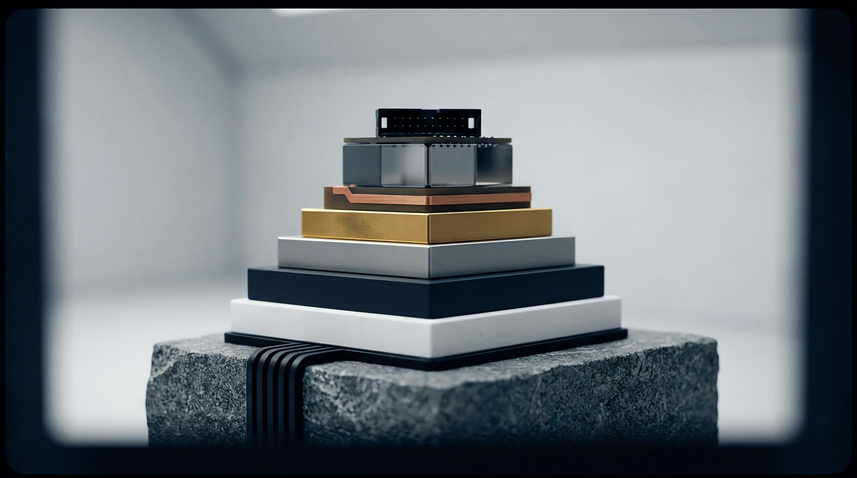
Passivation architectures separate environmental sealing from dielectric isolation and mechanical buffering. At the bottom, the primary layer sits against the semiconductor surface, where low interface trap density and high breakdown strength matter most. The intermediate layer provides bulk dielectric isolation and blocks moisture.
On top, an organic buffer absorbs packaging strain and defines solder-stop boundaries for flip-chip micro-bumps.

What Dictates Layer Sequence and Thickness Selection?
High-voltage switch operation leaves little margin on layer thicknesses. The base layer uses 15 to 30 nanometers of thermal silicon dioxide or ALD alumina to keep surface trap density down. Laying down thicker oxide here impedes heat transfer from the switch FET channel into adjacent metal heat sinks.
Because channel temperatures reach 150 degrees Celsius under continuous carrier drive, local thermal conductance cannot be sacrificed.
The secondary dielectric uses 300 to 600 nanometers of stoichiometric silicon nitride deposited by high-density plasma. This thickness halts mobile ion migration and withstands transient peaks up to 400 volts without punch-through. Above the nitride, 2.5 to 5.0 micrometers of photopatternable polyimide covers the die, etched only at bond pads.
This thick polymer keeps lossy epoxy mold compound outside the strong fringe fields near the switch gate fingers.
- Substrate surface cleaning with in-situ argon plasma strips native oxides and halogen residues before film growth.
- Interfacial dielectric deposition forms a low-defect boundary via thermal oxidation or atomic layer deposition.
- Bulk barrier nitride deposition grows dense silicon nitride using multi-frequency PECVD to balance film stress.
- Passivation patterning defines source, drain, and gate contact windows using anisotropic fluorine reactive ion etching.
- Polymer buffer application coats, soft-bakes, photolithographically patterns, and vacuum-cures the stress-relief overcoat.
Flip-chip attachment directly onto RF laminates requires flat polyimide pad openings. Uneven curing creates pad dishing, which skews solder joint volumes during high-speed automated placement.

Audit
Assessing passivation integrity requires stressing packaged switch assemblies under concurrent electrical and environmental loads. Standard DC breakdown checks miss traps that activate only under dynamic RF fields. Meaningful evaluation pairs high-temperature operating life tests with maximum rated RF power swept across all phase angles into a mismatched load.
Accelerated moisture testing combined with high RF carrier power reveals interfacial delamination before catastrophic short circuits occur.
Unbiased Highly Accelerated Stress Testing places modules in 130 degrees Celsius and 85 percent relative humidity at 2.3 atmospheres. Moisture reaching non-stoichiometric films reacts with unbonded silanol groups, creating conductive paths that degrade second harmonic performance. Regulatory limits from the Federal Communications Commission and European Telecommunications Standards Institute strictly cap out-of-band emissions at 1736 MHz and 2604 MHz for 868 MHz ISM hardware.
| Stress Test Protocol | Applied Conditions | Observable RF Metric Shift | Root Passivation Mechanism |
|---|---|---|---|
| High-Temperature Operating Life | 125 deg C, +35 dBm RF, 1000 hrs | Insertion Loss Rise > 0.2 dB | Channel Interfacial Trap Accumulation |
| Mismatch RF Ruggedness | 25 deg C, 10:1 VSWR, +37 dBm | Harmonic Level Rise > 12 dBc | Dielectric Micro-Breakdown at Drain Edge |
| Biased Moisture Exposure | 85 deg C, 85% RH, 50V DC Bias | Off-State Leakage Current Rise | Pinhole Water Ingress in Thin Nitride |
| Temperature Cycling | -40 to +125 deg C, 1000 cycles | Intermittent Switch Open Circuits | Polyimide Shear Delamination at Pad Edge |
Procurement teams review foundry qualification data for specific interfacial defect metrics. Broad Weibull distributions for dielectric breakdown justify lot rejections, as early failures indicate particle contamination during PECVD. Downstream module yields trace directly back to pinhole density in that primary dielectric layer.
Tariff
Passivation architecture drives wafer processing expense, assembly yield, and final component unit cost. Single-layer silicon nitride runs on standard CMOS lines at low cost, but its parasitic capacitance degrades switch isolation at high frequencies. Overcoming that loading requires widening FET peripheries, which consumes die area and drops the gross die per wafer.
Conversely, adding low-loss polymers like benzocyclobutene introduces mask steps, precursor costs, and dedicated spin tracks, raising front-end wafer fabrication expenses by 8 to 14 percent.
Sourcing choices depend on foundry geography and export trade classifications. Switches built on gallium arsenide or silicon-on-insulator carry specific export control classification numbers and duty rates tied to operating frequency and output power. Units rated over 10 watts peak draw closer customs scrutiny, where clearance holds quickly inflate inventory carrying costs for volume utility meter rollouts.
Suppliers sometimes swap out qualified dual-layer polymer stacks for cheaper single-layer nitride on price-sensitive RF bids. Incoming DC screening fails to catch the substitution. The failure mode surfaces two to three years into deployment, when outdoor condensation induces RF leakage across unbuffered dies and knocks utility meters offline.
Incoming qualification packets require cross-sectional scanning electron microscopy images documenting layer thicknesses alongside signed energy-dispersive X-ray spectroscopy data confirming film stoichiometry. Supply agreements lacking explicit chemical specifications leave buyers with little recourse when undocumented dielectric substitutions cause field failure rates to exceed acceptable thresholds.