Atomic Layer Deposition Passivation Basics for Quartz Resonator Stability
Sub-nanometer ALD alumina passivation prevents quartz electrode oxidation and surface adsorption, capping decade frequency drift below two parts per million.

Mass
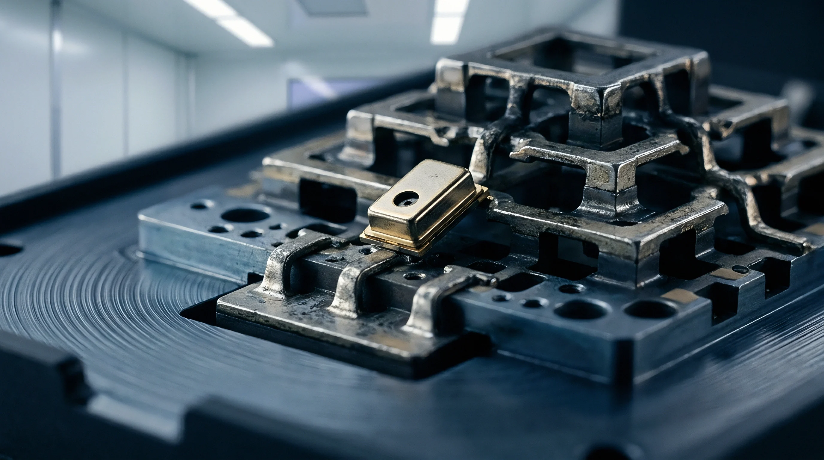
Maintaining frequency stability in piezoelectric quartz blanks requires a stable acoustic energy distribution across the active resonator region. Inside the package enclosure, unpassivated crystal surfaces interact constantly with ambient gas molecules, moisture, and volatilized organic compounds. This ongoing exchange alters the active crystal mass, triggering direct frequency shifts through piezoelectric mass loading ~ and causing unpassivated aluminum electrodes to degrade within months.
Surface mass accumulation relates to fundamental resonant frequency shift through the Sauerbrey formulation. Because frequency change scales inversely with active quartz area and density, microscopic mass additions on ultra-thin higher-frequency blanks trigger amplified frequency shifts. On a 26 MHz AT-cut crystal blank, even a single adsorbed monolayer of water shifts the resonant frequency by several parts per million, while oxidation steadily drives fundamental frequency drift downward.
Base metal electrodes ~ especially aluminum and silver alloys chosen for low electrical resistivity and favorable acoustic impedance matching ~ are inherently reactive. Over time, unpassivated aluminum forms native oxides that grow unevenly, consuming pure metal while altering the electrode’s thickness and density profile. Silver electrodes react with trace sulfur compounds to form silver sulfide structures, which introduce localized mechanical stress and raise acoustic dissipation.
| Electrode Material | Unpassivated Drift Rate (PPM Per Year) | Native Oxide Thickness (Nanometers) | Passivation Monolayer Target | Passivated Drift Rate (PPM Per Decade) |
|---|---|---|---|---|
| Aluminum (Pure 99.99%) | -4.8 to -8.2 | 3.5 to 5.0 | 2.0 nm Al2O3 | -0.3 to -0.6 |
| Silver-Copper Alloy | -6.1 to -12.5 | 4.0 to 8.5 | 3.0 nm Al2O3 / TiO2 | -0.4 to -0.8 |
| Gold (Chromium Underlayer) | -1.2 to -2.5 | 0.2 to 0.5 | 1.5 nm Al2O3 | -0.1 to -0.3 |
When a crystal oscillator operates at elevated temperatures, trapped volatile species detach from electrode surfaces and drive the resonant frequency higher. This dual directional behavior ~ mass adsorption during room-temperature storage versus desorption at high temperatures ~ complicates frequency compensation algorithms in long-range radios.
Unpassivated quartz crystal electrodes undergo irreversible frequency aging due to surface oxidation and continuous moisture adsorption.
In high-frequency fundamental resonators operating above 50 MHz, quartz blank thickness drops below thirty micrometers, allowing surface effects to dominate total crystal behavior. Microscopic asperities and chemical inhomogeneities on the crystal surface accelerate localized gas trapping. Without an atomic barrier layer, these surface dynamics erode narrow-band long-range link margins over operational lifespans beyond five years ~ and ignoring electrode surface chemistry risks product recalls when base station oscillators drift outside regulatory channel allocations after two years in the field.


Conformal
Atomic layer deposition relies on self-limiting chemical reactions to build uniform metal oxide dielectric barriers nanometer by nanometer across crystal surfaces. The process uses alternating pulses of precursor vapors separated by inert gas purges. Trimethylaluminum and water vapor act as primary precursors, depositing dense, amorphous aluminum oxide films that conform pinhole-free to the micro-topography of AT-cut and SC-cut quartz blanks.
Gas Reaction Mechanics and Self Limiting Growth
Gaseous precursor species enter the vacuum reaction chamber in sequential pulses under tight thermal control. The initial pulse delivers trimethylaluminum vapor, reacting with hydroxyl groups on the quartz blank and metal electrode surfaces. This surface reaction stops automatically once all available hydroxyl sites undergo chemisorption, forming a self-limiting monolayer before inert gas purges remove remaining vapor to prevent parasitic deposition.
After a nitrogen purge, a second pulse introduces water vapor into the chamber. Water molecules react with methyl groups bound to the aluminum atoms, creating strong aluminum-oxygen-aluminum bonds and releasing methane as a volatile byproduct. Repeating this sequence builds a dense dielectric film with sub-angstrom control per cycle, ensuring complete coverage over steep electrode step edges and surface micro-roughness.

Pinhole Damping and Dielectric Quality Limits
Acoustic shear wave dissipation increases when the deposited protective layer exceeds five nanometers in depth, dampening the resonator’s quality factor. Because quartz resonators store mechanical energy through high-Q acoustic shear modes, viscous or low-density dielectric coatings dampen oscillation and degrade phase noise performance. Consequently, the passivation layer must remain thin enough to prevent mechanical energy absorption while providing absolute gas impermeability.
Atomic layer deposition yields pinhole-free films at thicknesses down to fifteen angstroms ~ preventing drift where conventional physical or chemical vapor deposition methods require depths exceeding twenty nanometers to eliminate voids. The high density of atomic layer deposited alumina blocks oxygen and moisture diffusion into the underlying electrode metal without altering the resonator’s acoustic equivalent circuit parameters.
- Incomplete Chemisorption Nucleation Occurs when reactive hydroxyl groups on the quartz blank are insufficient, delaying local monolayer formation and leaving open diffusion paths to the electrode.
- Precursor Condensation Thermal Faults Arise when chamber temperatures fall below precursor condensation thresholds, causing multi-layer deposition that increases acoustic mass loading beyond target tolerances.
- Parasitic Gas Phase Reactions Occur when inter-pulse inert gas purges are too short, allowing reactive precursors to mix in the chamber and generate acoustic-damping particles.
- Pinholes From Surface Contamination Form when residual organic solvents stay on the quartz surface before processing, creating localized stress points and compromising the oxidation barrier.
A passivation layer exceeding three nanometers in thickness reduces crystal quality factor by increasing equivalent series resistance.
Because monolayer density dictates vapor barrier lifespan, process temperatures must be held between 100 degrees and 150 degrees Celsius to sustain high surface reaction kinetics without thermal-shocking delicate quartz mounting structures. Fabricators routinely attribute late-stage drift to post-packaging outgassing rather than addressing non-uniform precursor coverage inside reaction chambers.

Offset
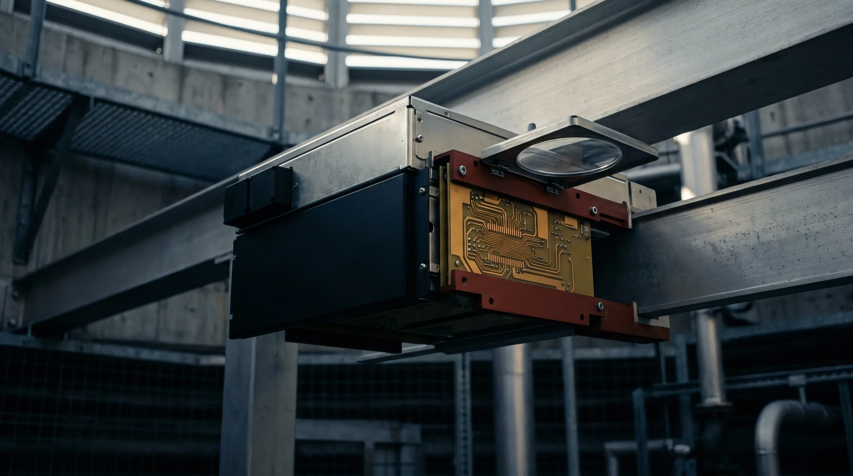
Carrier frequency deviation in a wireless transmitter degrades receiver sensitivity and increases packet error rates on long-range channels. When a quartz oscillator’s resonant frequency shifts from surface mass loading or electrode degradation, the RF synthesizer scales that error directly up to the carrier frequency: a 10 ppm drift in a 26 MHz reference crystal creates an 86.8 kHz offset in the 868 MHz ISM band, or 240 kHz at 2.4 GHz.
Where Does Passivation Damping Fail in High Humidity?
Moisture ingress through defective package seals deposits water onto exposed crystal electrodes, producing continuous frequency pull. In narrow-band protocols like LoRa, Sigfox, or NB-IoT, carrier offset forces the receiver channel filter off-center, reducing the effective signal-to-noise ratio. On a LoRa link running at 125 kHz bandwidth with spreading factor 12, an offset exceeding twenty-five percent of the bandwidth causes complete frame loss, destroying the link budget.
| Radio Protocol | Carrier Frequency | Max CFO Tolerance (PPM) | Sensitivity Loss at 10 PPM Drift (dB) | RX Window Expansion Penalty (%) |
|---|---|---|---|---|
| LoRaWAN (BW 125 kHz) | 868 / 915 MHz | +/- 15.0 | 3.5 | +185 |
| Bluetooth Low Energy 5.0 | 2.4 GHz | +/- 50.0 | 0.8 | +45 |
| NB-IoT (3GPP Rel 14) | 700 / 800 MHz | +/- 0.5 (Base Station Synchronized) | 5.2 | +210 |
| IEEE 802.15.4 (Zigbee) | 2.4 GHz | +/- 40.0 | 1.2 | +60 |
Low-power periodic sleep protocols like Bluetooth Low Energy or TSCH Zigbee rely on precise real-time clock oscillators to synchronize sleep-wake cycles between nodes, where carrier frequency offset degrades channel alignment. When oscillators drift, nodes must widen their preamble listen windows, directly increasing battery drain.
- Frequency Error Tolerances Define maximum allowable carrier offset before channel selection filters attenuate signals below demodulation thresholds.
- Preamble Detection Windows Require enlargement proportional to oscillator aging drift, directly driving up sleep-state energy draw in battery-powered field nodes.
- Channel Raster Guard Bands Must absorb worst-case multi-year frequency drift to prevent adjacent-channel interference in dense industrial deployments.
- Phase Noise Degradation Occurs when non-uniform passivation layers introduce mechanical damping, raising close-in phase noise and degrading higher-order quadrature modulation schemes.
A ten part per million crystal frequency drift expands required receiver preamble listen windows by more than one hundred percent in duty-cycled sensor networks.
An unpassivated oscillator drifting five parts per million annually forces firmware designers to build in wide timing margins, wasting milliamp-seconds of energy on idle listening. By contrast, an atomic layer passivated crystal holding drift under 0.5 ppm over ten years maintains low sleep currents. Over a device’s operating lifespan, receiver window expansion consumes far more energy than the initial cost of a passivated oscillator.
Stress
Thermal cycling induces structural strain across the interface between the inorganic oxide monolayer and the underlying metal electrode. Because thermal expansion coefficients differ substantially between AT-cut quartz blanks, aluminum or gold metallizations, and aluminum oxide protective layers, temperature swings generate interface shear displacement. These thermo-mechanical mismatches establish internal stress fields that alter the elastic constants of quartz through the stress-compensated piezoband effect.
Thermo Mechanical Shear across Substrate Interfaces
Differential expansion coefficients generate intrinsic lattice forces during temperature transitions. As temperatures rise from ambient to maximum operating limits, the metal electrode expands faster than the underlying quartz crystal while the rigid sub-nanometer oxide cap resists lateral movement. This shear strain gradient propagates into the active acoustic volume, shifting the fundamental resonant frequency independently of standard thermal expansion.
Accelerated life testing quantifies long-term stress relaxation and oxidation kinetics under elevated temperature and humidity. Applying Arrhenius models with activation energies specific to dielectric passivation layers enables evaluation of ten-year drift trajectories, while screening protocols validate stability under severe thermal gradient shocks.
- Maintain cleanroom chamber ambient pressure at ten to the power of negative four torr while stabilizing temperature at twenty-five degrees Celsius.
- Subject test quartz crystal resonators to five hundred consecutive thermal cycles ranging from minus forty degrees Celsius to plus one hundred twenty-five degrees Celsius with dwell times of fifteen minutes.
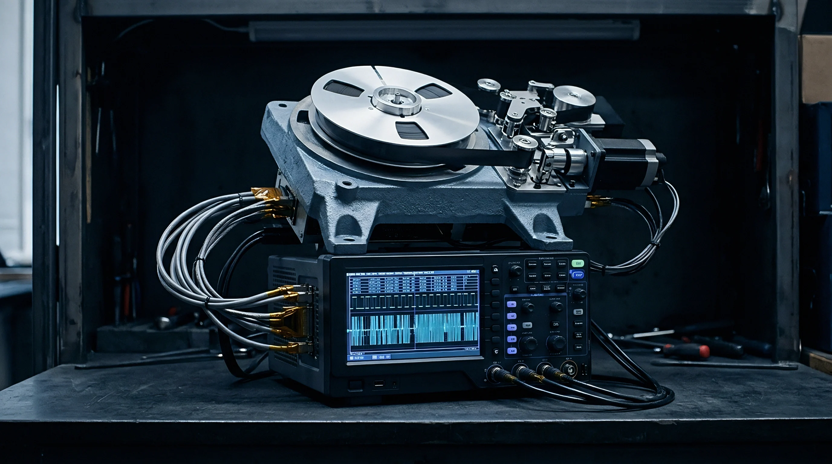
- Measure fundamental resonant frequency and equivalent series resistance every fifty cycles using a precision network analyzer driving crystals at rated drive levels.
- Expose thermal-shocked units to eighty-five percent relative humidity at eighty-five degrees Celsius for one thousand continuous hours to evaluate monolayer boundary degradation.
- Extract Arrhenius drift acceleration factors by comparing high-temperature frequency slope against ambient control sample baselines over three thousand hours.
Incomplete atomic monolayer nucleation creates stress concentration sites that accelerate micro-fracturing along electrode edges under thermal cycling.
Film stress can be engineered as compressive or tensile by adjusting precursor dwell times and deposition temperatures during atomic layer deposition cycles. Compressive films counteract the intrinsic tensile stress typical of evaporated aluminum electrodes, balancing the mechanical interface and stabilizing the crystal against thermal shock. Whether interfacial shear stress at sub-nanometer oxide boundaries relaxes linearly or logarithmically over decade deployment cycles remains an open empirical question across high-reliability crystal foundries.

Audit
Metrology screening verifies monolayer uniformity, oxide stoichiometry, and residual pinhole density prior to high-volume automated packaging. Validating atomic layer deposition coatings on quartz blanks requires surface analytical techniques with sub-nanometer spatial resolution, as conventional optical inspection cannot resolve dielectric layers below ten nanometers.
Spectroscopic Verification and Surface Layer Metrology
Spectroscopic Ellipsometry measures light polarization changes upon reflection from passivated crystal blanks to verify film uniformity, yielding precise thickness and refractive index profiles across entire wafer lots. Discrepancies in refractive index point to non-stoichiometric oxide formation or trapped precursor residues, signaling compromised barrier performance.
Transmission Electron Microscopy cross-sectional analysis provides direct physical visualization of the oxide-electrode interface. High-resolution TEM confirms atomic-level conformity across crystal edge steps and establishes exact layer thickness. Combined with X-ray Photoelectron Spectroscopy, auditors quantify atomic ratios of aluminum to oxygen, confirming full oxidation without residual carbon contamination from precursor methyl groups.
| Inspection Method | Measured Parameter | Resolution Limit | Production Suitability | Failure Detection Capability |
|---|---|---|---|---|
| Spectroscopic Ellipsometry (SE) | Film thickness, Refractive index | 0.1 nm | 100% Inline Wafer Automated | Thickness variance, Density loss |
| X-Ray Photoelectron Spectroscopy (XPS) | Chemical stoichiometry, Impurities | 0.5 atomic % | Destructive Batch Sampling | Unreacted carbon, Sub-oxides |
| Atomic Force Microscopy (AFM) | Surface roughness, Pinholes | 0.05 nm vertical | Batch Qualification Screening | Micro-voids, Grain boundaries |
| Transmission Electron Microscopy (TEM) | Lattice interface, Layer boundary | 0.01 nm | Failure Analysis Only | Interface delamination, Voiding |
Because spectral compliance demands narrow frequency tolerances, sourcing specifications must mandate verification protocols that test passivated crystals under combined electrical drive level stress and humidity exposure. Suppliers providing raw crystal blanks without atomic layer passivation introduce unquantified aging risks into downstream radio modules.
Batch verification using spectroscopic ellipsometry catches monolayer thickness deviations across quartz wafer surfaces before dicing and assembly operations.
Audit dossiers must include spectroscopic proof of film density alongside standard frequency tolerance metrics. Mandating compliance with recognized component qualification standards ensures long-term crystal oscillator reliability across outdoor industrial wireless deployments. Specifically, compliance with MIL-PRF-3098 Section 4.8.2 forces vendors to submit batch spectral stability measurements taken after three hundred thermal shock cycles.