Trap Rich Polysilicon Layer Optimization for Harmonic Suppression in Front End Modules
Trap rich polysilicon layers freeze interface charges to hold high resistivity and suppress switch harmonics below minus eighty dBc.
Substrate
When high-power radio frequency signals pass through silicon-on-insulator switch networks, the resulting electric fields penetrate the buried dielectric layer. In standard high-resistivity silicon handles with bulk resistivities above one thousand ohm centimeters, fixed positive charges inside the silicon dioxide insulator pull in mobile charge carriers, forming an electrical inversion or accumulation layer directly beneath the dielectric interface. As alternating RF voltages up to thirty-six dBm drive overlying field-effect transistors, the alternating field modulates mobile charge density across this interface zone.
This dynamic modulation creates nonlinear, voltage-dependent capacitance and conductance that distort high-amplitude RF signals, generating severe harmonics and intermodulation products that degrade overall module performance.
Inserting an engineered polysilicon film between the single-crystal silicon base and the buried oxide layer stops this physical degradation. The polycrystalline film features a dense network of grain boundaries and structural defects that act as high-density deep-level electronic traps. These traps capture mobile electrons and holes before they can move under strong AC electric fields, dropping recombination lifetimes to picoseconds rather than microseconds.
By immobilizing mobile carriers, the polycrystalline film prevents conductive interface channels from forming and holds the effective substrate resistivity above ten thousand ohm centimeters ~ even under thirty-six dBm signal excitation where strong voltage swings would otherwise sweep substrate charge across the interface.

Parasitic Surface Conduction Mechanics
Fixed positive charges in buried thermal oxides pull mobile electrons toward the upper boundary of the handle wafer, concentrating charge carriers within a thin layer roughly ten to fifty nanometers deep. This localized electron concentration drops surface resistivity from several thousand ohm centimeters down to less than ten ohm centimeters. Under small-signal conditions, this conductive path introduces moderate parasitic insertion loss along RF transmission lines; under large-signal drive, the spatial distribution of charge expands and contracts in step with the applied RF voltage cycle.
Modulating this mobile charge under high RF drive produces a non-monotonic capacitance curve when measured across sweeping DC and AC voltages. On positive voltage peaks, extra electrons are drawn to the interface, boosting parallel capacitance. When the voltage swings negative, these electrons deplete, shifting the capacitive coupling path into the handle wafer.
This dynamic variation creates sharp current spikes at integer multiples of the fundamental frequency. Third-order harmonic components generated this way scale rapidly, rising three decibels for every single decibel increase in fundamental input power.
Free carrier accumulation at the buried oxide interface creates voltage-dependent capacitance that drives intermodulation distortion.
Buried Oxide Interface Field Distribution
Alternating voltages across switch nodes drive potential lines down through the silicon dioxide dielectric, where peak RF power levels can push electric field strength inside the oxide beyond one megavolt per centimeter. These intense fields penetrate the upper fifty nanometers of the silicon substrate, directly driving carrier dynamics. Without a high density of electronic traps, the electric field readily displaces mobile electrons and redistributes charge along the interface plane.
Field penetration depth depends on signal frequency, dielectric thickness, and local free-carrier concentration. At cellular frequencies between seven hundred megahertz and six gigahertz, the RF field reaches well into the handle silicon, establishing an active conduction volume. Placing a disordered polycrystalline film beneath the oxide absorbs these field lines across a dense network of defects, where deep acceptor and donor energy states clamp the electrostatic potential and stop field-induced carrier modulation in the underlying single-crystal base.
Nonlinear Capacitance and Intermodulation Generation
Voltage-dependent charge accumulation alters local differential permittivity during power peaks. When two separate frequency tones pass through a front-end switch together, this nonlinear capacitance mixes them, creating intermodulation products ~ including third-order tones that land straight inside adjacent receive bands. In multi-band cellular systems, these third-order products desensitize low-noise amplifiers, degrading noise figures and eating into the overall link budget.
Measuring second and third harmonic power across coplanar waveguide test structures quantifies the magnitude of this nonlinear distortion. While an un-passivated substrate generates third-harmonic spurs exceeding minus sixty-five dBc at thirty-three dBm input power, adding a polycrystalline trap film pulls those spurious emissions below minus ninety dBc under identical drive conditions. Holding this degree of suppression across operating temperatures up to one hundred and twenty-five degrees Celsius requires precise control over the energy distribution of defect states within the polycrystalline layer.
- Buried Oxide Interface Accumulation Fixed positive charges inside thermal oxides attract free electrons, forming a localized conductive layer that reduces surface resistivity beneath switch nodes.
- Voltage Dependent Capacitance Modulation Alternating RF electric fields alter the interface charge layer depth, creating nonlinear capacitive paths that distort high-amplitude transmit signals.
- Harmonic Frequency Generation Dynamic carrier displacement under high signal drive generates second and third harmonic emissions that exceed regional carrier compliance limits.
- Intermodulation Products Distortion Two-tone signal mixing across nonlinear substrate capacitance produces spurious in-band noise that blinds adjacent low-noise receiver circuits.
Failing to suppress parasitic surface conduction degrades third-harmonic margin by twenty decibels, leaving cellular switch modules non-compliant against regional carrier emission specifications.

Grain
Polycrystalline microstructures deposited between single-crystal handle wafers and dielectric boundaries create dense trap distributions. Within these films, small crystalline domains are separated by highly disordered grain boundary regions where un-passivated dangling silicon bonds and structural dislocations concentrate. These physical defects create energy states deep within the bandgap of the silicon lattice, pinning the Fermi level near mid-gap and restricting the movement of both conduction-band electrons and valence-band holes.
Microstructural grain size directly sets the volume density of grain boundaries. Reducing average grain size from two hundred nanometers down to thirty nanometers increases grain boundary surface area by nearly an order of magnitude. This finer grain structure yields trap densities exceeding ten to the nineteenth traps per cubic centimeter, capturing free carriers so quickly that carrier lifetimes drop below one picosecond.
Controlling grain nucleation and growth during film deposition is therefore critical to maintaining high trap density through later thermal steps.
Boundary Trapping Energy States
Dangling atomic bonds along disordered boundaries form localized electron and hole capture centers near mid-gap. These energy states feature broad thermal capture cross-sections for mobile carriers. When an RF electric field injects electrons into the polycrystalline film, these mid-gap states capture them before they can contribute to macroscopic conduction, keeping charges immobilized within deep states throughout the RF signal half-cycle.
The energy distribution of these traps includes both neutral donor and neutral acceptor levels across the bandgap. Acceptor-like states in the upper half of the bandgap trap excess electrons to become negatively charged, while donor-like states in the lower half capture excess holes to become positively charged. Balancing these occupied donor and acceptor states maintains electrical neutrality, preserving an effective substrate resistivity above ten thousand ohm centimeters under heavy RF stress.
Deposition Parameters and Microstructure Control
Low-pressure chemical vapor reactors regulate silane pyrolysis temperatures to control crystal nucleus formation. Depositing silicon films between five hundred and forty and five hundred and eighty degrees Celsius produces an initial amorphous or semi-amorphous matrix. Subsequent low-temperature annealing converts this matrix into a fine-grained polycrystalline film with a uniform boundary distribution, securing fine grain boundaries before subsequent thermal exposure can drive grain growth and destroy defect states.
| Deposition Process | Temperature Range | Average Grain Size | Trap State Density | Effective Resistivity |
|---|---|---|---|---|
| Low Pressure Chemical Vapor Deposition | 540 deg C to 560 deg C | 20 nm to 40 nm | 2.5 x 10^19 cm^-3 | 18,000 ohm cm |
| Low Pressure Chemical Vapor Deposition | 580 deg C to 600 deg C | 60 nm to 100 nm | 8.0 x 10^18 cm^-3 | 12,000 ohm cm |
| Low Pressure Chemical Vapor Deposition | 620 deg C to 640 deg C | 150 nm to 250 nm | 1.2 x 10^18 cm^-3 | 3,500 ohm cm |
| Plasma Enhanced Chemical Vapor Deposition | 400 deg C to 450 deg C | 10 nm to 25 nm | 3.1 x 10^19 cm^-3 | 22,000 ohm cm |
Direct deposition above six hundred and twenty degrees Celsius yields coarse columnar grain structures with average sizes exceeding two hundred nanometers, drastically cutting total boundary volume. These coarse grains provide lower trap density, allowing free-carrier conduction channels to form beneath the oxide during high-voltage RF drive. Selecting deposition pressures between zero point two and zero point eight Torr optimizes silane decomposition rates, ensuring uniform nucleation across entire three-hundred-millimeter wafers.
An effective resistivity exceeding ten thousand ohm centimeters requires a trap density above ten to the nineteenth per cubic centimeter under thirty-three dBm RF drive.

Fermi Level Pinning at Crystal Interfaces
A high density of deep defect sites forces the equilibrium Fermi level toward mid-gap. Pinning the Fermi level near zero point five six electron volts above the valence band edge keeps the film from developing strong n-type or p-type conductivity. Even if background dopants like boron or phosphorus contaminate the layer during processing, the high trap density absorbs them without shifting the Fermi level.
This Fermi level pinning keeps carrier concentrations in the polycrystalline layer near the intrinsic limit of roughly ten to the tenth per cubic centimeter, yielding film resistivities above one hundred thousand ohm centimeters. The high trap density prevents external electric fields from pulling the Fermi level toward the conduction or valence band edges, stabilizing the layer energetically to ensure linear RF performance across sweeping temperatures and variable DC bias.
At low signal levels, grain coarsening during front-end oxidation can appear to remain well within standard electrical limits.


Thermal
High-temperature front-end manufacturing drives structural relaxation inside disordered silicon films. Standard CMOS steps ~ thermal oxidation, dopant drive-in, and film annealing executed between nine hundred and eleven hundred degrees Celsius ~ provide high thermal energy that accelerates atomic diffusion. Silicon atoms along grain boundaries realign into lower-energy lattice positions, causing small microscopic grains to coalesce into larger single-crystal domains.
This grain coarsening reduces total grain boundary surface area and destroys deep-level trap states. As thermal budgets accumulate through front-end processing, trap density can drop below the threshold needed to freeze parasitic surface conduction. Because the overall thermal budget dictates grain stability, preserving high effective resistivity requires techniques that suppress grain growth kinetics during high-temperature steps ~ such as introducing atomic grain-growth inhibitors or using post-deposition defect engineering.
Recrystallization Kinetics during High Temperature Steps
Annealing steps above nine hundred degrees Celsius activate grain growth pathways that eliminate defect boundaries. Silicon self-diffusion along grain boundaries carries an activation energy near two point three electron volts. When processing temperatures exceed one thousand degrees Celsius for extended periods, thirty-nanometer fine grains quickly grow beyond one hundred and fifty nanometers, reducing volumetric trap state density by more than eighty percent.
In bench characterization of coplanar waveguide test structures, high-temperature process duration correlates directly with lost harmonic performance. Subjecting a trap-rich substrate to a ten-hour, eleven-hundred-degree oxidation cycle degrades effective resistivity from fifteen thousand ohm centimeters down to less than two thousand ohm centimeters. That drop drives a fifteen-decibel increase in third harmonic emissions under thirty-three dBm input drive, making strict control over total thermal budget during module fabrication essential.

Ion Implantation for Defect Preservation
Bombarding the lattice network with heavy species introduces stable atomic displacement damage prior to thermal oxidation. Implanting neutral argon or silicon ions creates amorphized zones and point defect clusters throughout the polycrystalline film, where argon ions act as physical pinning sites that block grain boundary migration during high-temperature steps.
Injecting argon ions at doses between ten to the fourteenth and ten to the fifteenth ions per square centimeter creates stable interstitial defect complexes that stabilize defect density against thermal annealing. Because these ion-induced defects carry high activation energy barriers, implant-stabilized films retain trap densities above ten to the nineteenth per cubic centimeter even after one-thousand-degree thermal cycles, preventing parasitic surface conduction under high RF fields.

Wafer Stress and Mechanical Bow Control
Differences in thermal expansion coefficients between oxide layers and thick polycrystalline films generate mechanical stress that alters wafer curvature. Depositing polycrystalline films thicker than two micrometers introduces compressive stress that causes significant wafer bow. When bow exceeds thirty micrometers across a three-hundred-millimeter disk, it leads to photolithographic focus errors and handling failures in automated toolsets.
Keeping film thickness between zero point five and one point five micrometers strikes a balance between electrical trap performance and mechanical stress limits. These thinner films keep mechanical bow below fifteen micrometers, ensuring full compatibility with advanced steppers and scanners. Fine-tuning deposition pressure and annealing ramp rates further lowers residual stress, maintaining wafer planarity through front-end manufacturing.
- Deposition of zero point eight micrometer amorphous silicon layer via LPCVD at five hundred and fifty degrees Celsius.
- Implantation of argon ions at an energy of one hundred and eighty kiloelectron volts with a dose of five times ten to the fourteenth per square centimeter.
- Initial solid-phase crystallization anneal executed at six hundred and fifty degrees Celsius for two hours under high-purity nitrogen ambient.
- Buried oxide bonding thermal cycle performed at nine hundred and fifty degrees Celsius to form the primary silicon-on-insulator stack.
- Front-end-of-line CMOS transistor fabrication steps operating within a cumulative thermal budget limit below ten hours at one thousand degrees Celsius.
- Post-process inline RF coplanar waveguide second harmonic extraction to verify thermal stability of the underlying trap layer.
Whether argon ion amorphization can fully survive extreme high-temperature CMOS drive-in steps without creating localized pinhole leakage paths across the dielectric boundary remains an open question.

Harmonics
Nonlinear distortion products from front-end switches compromise receiver sensitivity. In modern multi-mode cellular transceivers operating under 5G NR FR1 specifications, power amplifiers transmit at high power while low-noise amplifiers simultaneously listen for weak signals. When transmit switches generate spurious harmonics, that energy leaks into adjacent receive bands, elevating the noise floor and degrading the signal-to-noise ratio.
Optimized polycrystalline trap films suppress second and third harmonic emissions across cellular bands from seven hundred megahertz to seven point one two five gigahertz, as well as Wi-Fi 6E and Wi-Fi 7 bands up to seven point two gigahertz. Eliminating parasitic surface conduction keeps second harmonic distortion below minus eighty-five dBc and third harmonic distortion below minus ninety-five dBc at thirty-five dBm RF drive. Maintaining this linearity prevents self-interference from transmit signals, protecting link budgets in high-data-rate wireless modules.
Second and Third Harmonic Roll off Characteristics
Spurious frequency components scale nonlinearly as RF conduction currents grow across high-power transmit paths. On un-trapped substrates, second harmonic power increases quadratically with fundamental input power, while third harmonic power rises cubically. Adding a high-density polycrystalline trap layer changes this scaling behavior, pushing harmonic output down into the thermal noise floor across normal operating power levels.
When measuring second and third harmonic power across a frequency sweep from one to six gigahertz, trap-rich substrates maintain a flat, low-level response. Suppression remains consistent across both low-band cellular frequencies near eight hundred megahertz and high-band Wi-Fi frequencies at six gigahertz, avoiding the receiver margin degradation caused by phase noise. Freezing free carriers prevents high-frequency electric field modulation, ensuring linear transmission across all assigned spectrum bands.
Compliance with 3GPP TS 38.101 harmonic limits forces module manufacturers to guarantee second harmonic rejection below minus thirty-six dBm.
Intermodulation Suppression under High RF Power
Two-tone excitation tests under thirty-three dBm drive reveal mixing products created by voltage-dependent substrate capacitance. When two transmit signals at frequencies f1 and f2 pass through a nonlinear switch, their interaction generates third-order intermodulation products at two f1 minus f2 and two f2 minus f1. Because these products often fall directly inside active receive channels, physical filtering is impossible once they form.
| Substrate Architecture | Frequency Band | HD2 Suppression | HD3 Suppression | IMD3 Level |
|---|---|---|---|---|
| Standard High Resistivity Silicon | Cellular Band n77 (3.7 GHz) | -68 dBc | -62 dBc | -82 dBc |
| Basic Un-implanted Trap Layer | Cellular Band n77 (3.7 GHz) | -82 dBc | -84 dBc | -98 dBc |
| Argon Implanted Trap Layer | Cellular Band n77 (3.7 GHz) | -92 dBc | -98 dBc | -108 dBc |
| Standard High Resistivity Silicon | Wi-Fi 6E Band (6.5 GHz) | -64 dBc | -58 dBc | -78 dBc |
| Argon Implanted Trap Layer | Wi-Fi 6E Band (6.5 GHz) | -88 dBc | -94 dBc | -104 dBc |
Integrating an argon-implanted polycrystalline trap layer reduces third-order intermodulation products below minus one hundred and eight dBc. In RF switch harmonic sweeps, intermodulation suppression improves by twenty-six decibels over standard high-resistivity silicon handles. This performance gap widens further as operating temperatures reach one hundred and twenty-five degrees Celsius, demonstrating the thermal stability of mid-gap energy trap states.
Why Do Harmonic Spurs Persist under RF Stress?
High peak voltage amplitudes can drive mobile carriers beyond localized trap emission rates, allowing transient conduction channels to form. When peak-to-peak RF voltage swings across a switch node exceed forty volts, local electric field peaks surpass the breakdown thresholds of fine grain boundaries. Under this stress, captured carriers gain enough thermal energy to escape deep traps, temporarily re-establishing an interfacial conduction path.
Trapping rate dynamics dictate how rapidly trapped carriers recombine relative to the RF period. If the detrapping time constant aligns with the RF period, transient charge accumulates and produces persistent harmonic spurs. Optimizing grain boundary energy distributions through argon implantation creates deeper potential wells that extend detrapping times far beyond the RF period.
This locks carriers in place and shortens carrier lifetimes near boundaries, suppressing transient harmonic generation during maximum transmit power bursts.
Section 4.2 of standard carrier qualification requirements sets an absolute third-order intermodulation limit of minus one hundred and five dBm under thirty-six dBm peak transmit power, forcing front-end module vendors to guarantee minimum trap densities.

Probing
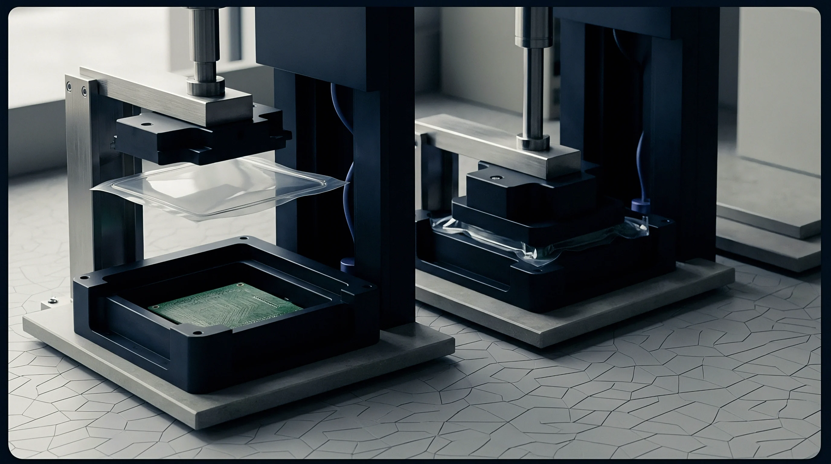
Inline characterization measures effective resistivity and spurious signal generation directly on patterned silicon. Traditional four-point probe DC tests fail to capture the high-frequency surface conduction dynamics that drive RF harmonic generation; DC resistivities above ten thousand ohm centimeters can easily mask severe carrier accumulation under buried thermal oxides. Evaluating trap-rich substrates therefore requires advanced RF test vehicles and high-frequency characterization methods run directly on production wafers.
Coplanar waveguide transmission lines, RF capacitance-voltage profiling, and transient microwave photoconductive decay measurements yield quantitative metrics of substrate quality. Extracting second harmonic power across a standard coplanar line gives a direct, calibrated measurement of effective substrate linearity. Automated wafer-level RF probing then enables full-map characterization, isolating defective substrate zones before wafers move into costly front-end fabrication.
Coplanar Waveguide Transmission Line Test Structures
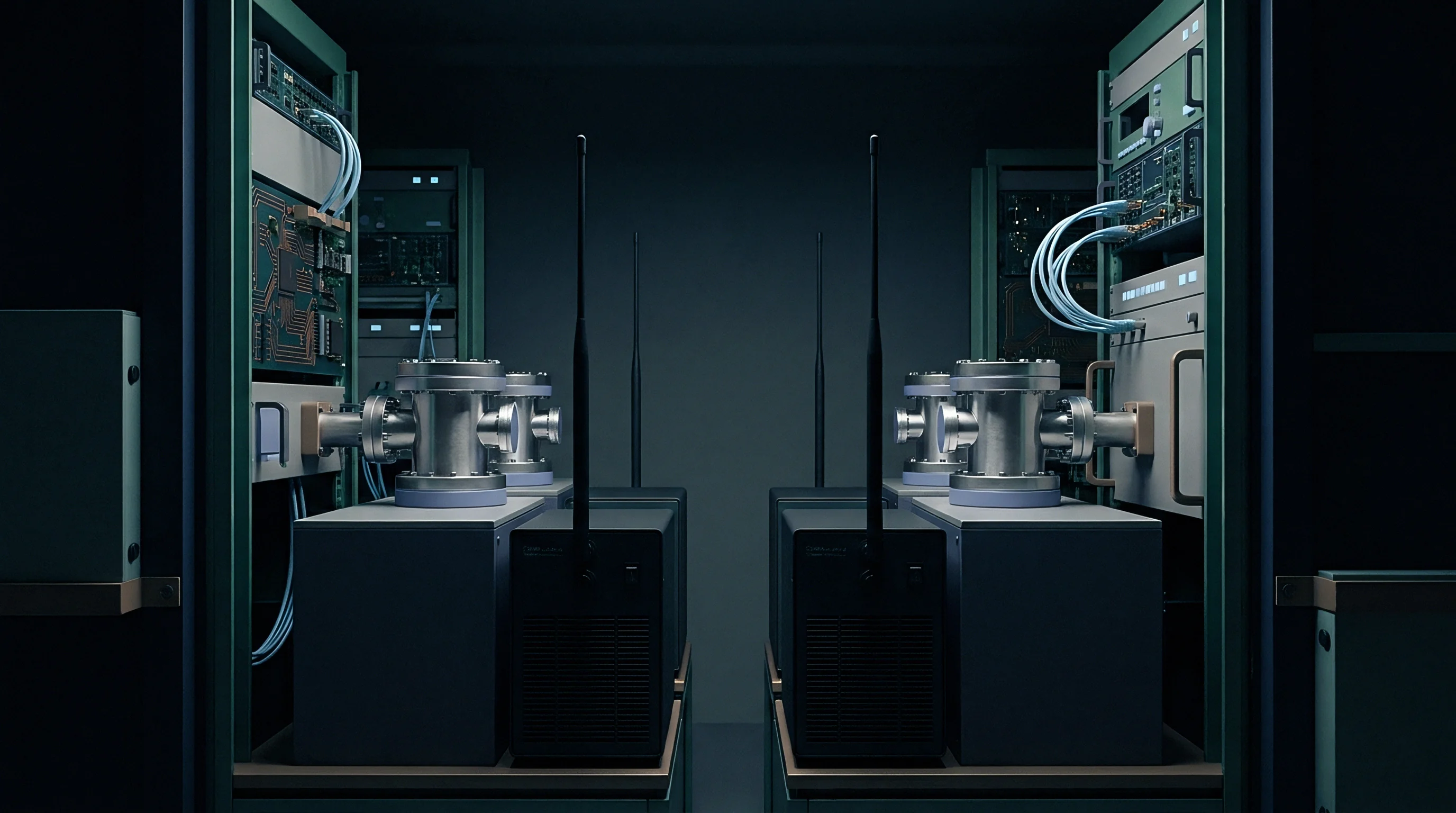
Integrated RF test vehicles use ground-signal-ground metallization topologies fabricated directly over trap layers. A standard coplanar waveguide structure features a twenty-micrometer signal line separated from parallel ground planes by a fifteen-micrometer gap. Passing a high-power microwave signal through this line concentrates intense electric fields within the underlying substrate interface.
Measuring insertion loss and second harmonic output from one to twenty gigahertz allows direct calculation of effective substrate resistivity. Un-passivated surface conduction layers introduce high transmission line attenuation ~ exceeding zero point five decibels per millimeter at six gigahertz ~ while high-quality trap-rich substrates keep attenuation below zero point one decibel per millimeter, confirming that free-carrier conduction paths are fully suppressed.
RF Capacitance Voltage Profiling and Extraction
High-frequency admittance measurements across swept DC bias voltages isolate interface state density from substrate doping. By applying a one-megahertz AC signal while sweeping DC bias from minus fifty to plus fifty volts, engineers extract the differential substrate capacitance curve to evaluate how trap passivation shifts energy states and how defect density governs harmonic performance.
A flat capacitance-voltage curve across wide DC bias sweeps confirms that interface charge accumulation is suppressed. Substrates without sufficient trap density show steep, asymmetric capacitance peaks as the DC voltage draws mobile electrons into accumulation or inversion layers. Calculating the derivative of the capacitance-voltage curve provides a fast inline metric for screening incoming wafer lots.

Transient Microwave Reflectivity and Lifetimes
Laser-induced optical excitation generates minority carriers while microwave absorption decay rates track trap recombination velocity. An ultra-short optical pulse generates free electron-hole pairs within the top micrometer of the substrate, and a focused microwave probe beam monitors the transient decay of these carriers in real time.
In substrates with high trap boundary densities, optically injected carriers recombine almost instantaneously, yielding microwave reflectivity decay times below two picoseconds. Substrates with degraded trap densities exhibit prolonged decay times lasting several nanoseconds. Automated transient reflectivity tools scan three-hundred-millimeter wafers in minutes, generating spatial carrier lifetime maps that predict final module harmonic yield.
Thicker trap layers improve harmonic margin until mechanical substrate bow compromises backend photolithography.
- Coplanar Waveguide Harmonic Screening Measuring second harmonic power generated across standard coplanar line vehicles verifies substrate linearity under thirty-three dBm drive.
- Swept Voltage Capacitance Profiling Extracting admittance curves across wide DC bias ranges identifies transient carrier accumulation peaks beneath buried oxide layers.
- Transient Optical Decay Mapping Monitoring microwave reflectivity decay times following pulsed optical excitation quantifies minority carrier recombination velocity.
- Wafer Level Effective Resistivity Extraction High-frequency S-parameter extraction isolates effective substrate resistivity values from parasitic transmission line loss.
High-frequency capacitance-voltage curves with a flat differential slope across negative and positive voltage sweeps reliably indicate effective carrier suppression.

Sourcing
Foundry procurement contracts for engineered RF-SOI substrates establish strict structural and electrical qualification limits. Front-end module manufacturers source engineered handle wafers from specialized silicon suppliers operating proprietary bonding and trap-layer deposition lines. Maintaining consistent RF switch performance across high-volume production runs requires embedding precise structural specifications directly into wafer purchasing agreements.
Substrate specifications set target values for polycrystalline film thickness, argon implantation dose, minimum trap density, maximum allowable wafer bow, and effective RF resistivity. Adding a trap-rich layer increases raw wafer cost by fifty to ninety dollars per three-hundred-millimeter disk. Weighing this premium against final module packaging yields, harmonic compliance margins, and carrier pass rates easily justifies the investment for high-performance cellular and Wi-Fi markets.
Wafer Substrate Ecosystem and Foundry Procurement
Raw silicon vendors deliver engineered handle material through certified bonding lines under strict quality protocols. The global supply chain for trap-rich RF-SOI substrates relies on a small group of specialized fabricators capable of producing three-hundred-millimeter wafers. Because wafer bow exceeding thirty micrometers causes measurable landed yield losses, procurement teams enforce strict mechanical incoming inspection standards.
Substrate buyers negotiate supply contracts combining handle wafer specifications with buried oxide thickness targets. Standard front-end module architectures pair a buried oxide layer zero point two to zero point four micrometers thick with an underlying trap layer of zero point eight to one point two micrometers. Securing multi-year contracts with second-source suppliers requires cross-qualifying trap-layer deposition processes across different commercial foundry lines.
Specification Tolerances and Quality Agreements
Technical supply contracts specify maximum allowable local bow, interface charge density, and minimum effective resistivity. Quality agreements require incoming wafer lots to undergo inline RF testing before release to production lines, while qualification clauses set statistical process control limits for harmonic emissions measured on test coupons.
| Procurement Parameter | Standard Specification | Tight Quality Tolerance | Impact of Out of Spec Parameter |
|---|---|---|---|
| Polycrystalline Layer Thickness | 0.80 um +/- 0.10 um | 0.80 um +/- 0.03 um | Wafer bow increase or reduced trap volume |
| Minimum Bulk Trap Density | 1.0 x 10^19 cm^-3 | 2.5 x 10^19 cm^-3 | Increased HD3 harmonic spurs under drive |
| Maximum Wafer Mechanical Bow | < 30 micrometers | < 15 micrometers | Lithographic defocus during front-end processing |
| Argon Implantation Dose | 5.0 x 10^14 cm^-2 | 5.0 x 10^14 +/- 5% | Grain growth during high-temp drive-ins |
| Effective RF Resistivity | > 10,000 ohm cm | > 18,000 ohm cm | Excessive coplanar transmission line loss |
Because wafer warpage degrades lithographic yield, rejecting incoming wafer lots that fail effective resistivity thresholds prevents high processing costs on non-compliant silicon. Procurement agreements typically specify that if more than two percent of test coupons in a single lot exhibit third harmonic suppression worse than minus eighty-five dBc, the entire shipment is subject to commercial return and credit.

Landed Cost and Yield Arithmetic
Adding advanced polycrystalline trap layers increases prime substrate cost by forty to ninety dollars per three-hundred-millimeter disk. A standard high-resistivity silicon-on-insulator wafer costs roughly four hundred and fifty dollars, compared to five hundred to five hundred and forty dollars for an optimized trap-rich substrate. For a high-volume front-end module yielding two thousand dies per wafer, this premium translates to an added raw material cost of two point five to four point five cents per die.
When evaluated against module qualification metrics, this initial cost premium protects overall profitability. Non-passivated substrates experience final RF test failure rates exceeding twelve percent due to harmonic emission spikes during carrier compliance testing, whereas optimized trap-rich substrates drop harmonic test failure rates below zero point two percent. Protecting final package yield avoids substantial backend packaging and test costs, delivering a clear net positive return on the engineered wafer investment.
Engineers evaluating commercial front-end module yields track interface defect density alongside thermal processing history to verify substrate reliability before releasing high-volume masks.