Nanolaminate Atomic Layer Deposition Interfacial Shear Stress Kinetics under High Power Transmit Cycling
Nanolaminate ALD passivations resist cyclic shear stress during RF transmit bursts when individual sub-layer thicknesses remain below critical slip limits.

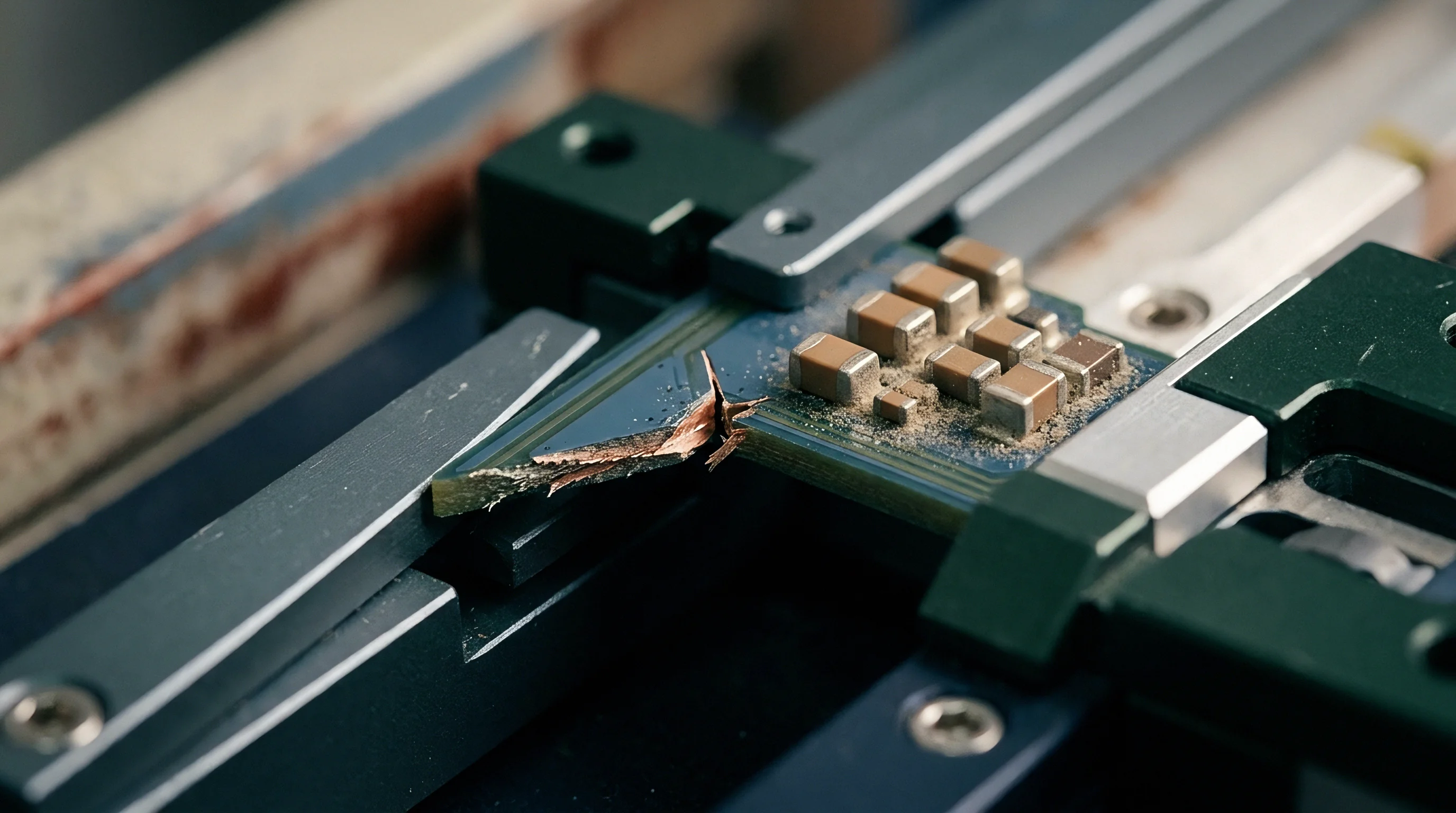
Stack
Atomic layer deposition coats gallium nitride and gallium arsenide radio frequency power dies with alternating oxide nanolaminates to halt moisture penetration and suppress surface trap states. Alternating sub-nanometer lamellae of aluminium oxide and titanium dioxide or zirconium dioxide provide dielectric passivation across high-electron-mobility transistor mesas. High power transmit pulses drive rapid thermal transients into these dielectric coatings.
When a cellular transceiver enters Class 2 high power user equipment operation at thirty-one decibels relative to one milliwatt, or when a private data terminal pushes five watts through an external front-end module, the metal-dielectric boundary absorbs cyclic mechanical loads.
Alternating thin films distribute internal elastic strain across sub-layer boundaries rather than concentrating stress at a single substrate junction.
Each transmit burst produces a rapid heat flux within the transistor active channels. The underlying gold, copper, or aluminium transmission lines expand against the amorphous oxide barrier. Gallium nitride presents a thermal expansion coefficient near 5.6 parts per million per Kelvin, while gold conductors expand at 14.2 parts per million per Kelvin.
The amorphous aluminium oxide layers sit near 7.0 parts per million per Kelvin, and titanium dioxide phases range between 8.0 and 9.5 parts per million per Kelvin. Although alumina resists creep, this physical expansion disparity generates intense cyclic shear loads across the laminate planes during microsecond-scale radio bursts.
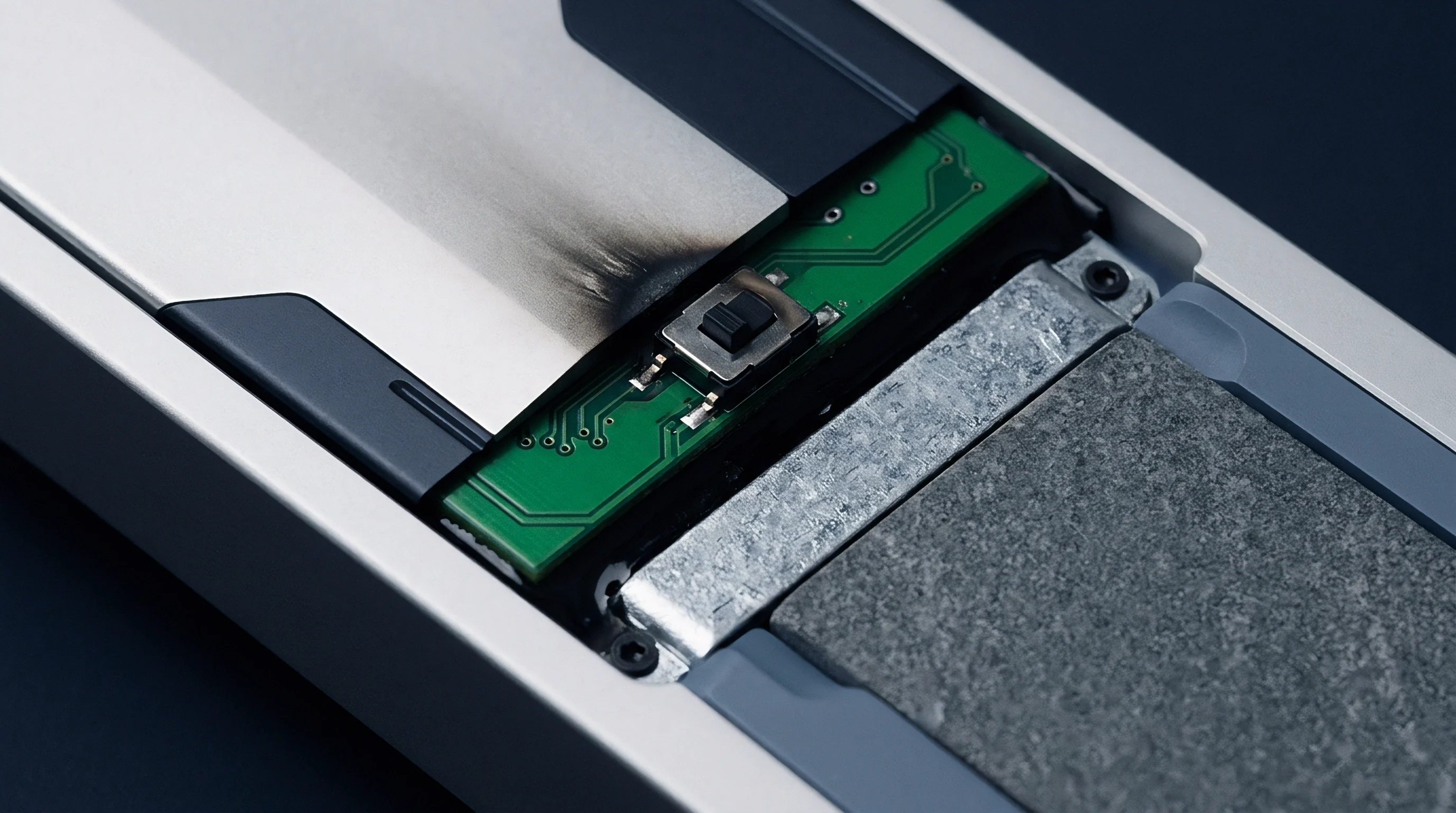
Nanolaminate Dielectric Architecture in RF Modules
Dielectric coatings composed of single thick oxide layers develop through-thickness cracks under sustained radio frequency drive levels. Depositing alternating layers with individual thicknesses between two and fifteen nanometers forces microcracks to deflect along internal interfaces. An aluminium oxide layer grown via trimethylaluminium and water vapor provides electrical isolation and adhesion.
A subsequent layer of zirconium dioxide or hafnium dioxide deposited from alkylamide precursors supplies dielectric density and environmental impermeability. The combined multi-layer barrier maintains a total thickness between fifty and two hundred nanometers across the active transistor fingers.
Total layer count governs the density of shear-deflecting planar boundaries. Increasing the laminate count from four bilayers to sixteen bilayers reduces individual layer thicknesses toward molecular dimensions. Thinner sub-layers alter the local yield behavior from bulk slip to constrained interfacial shearing.
The critical shear stress required to induce plastic displacement within the laminate scales inversely with the square root of the individual layer thickness. Thinner lamellae hold higher peak elastic strains before initializing slip along the metal contact interfaces.
Interfacial Shear under Pulsed Transmit Cycling
Pulse width governs strain. In Time Division Multiple Access transmissions, typical pulse durations range from five hundred microseconds to several milliseconds. Long pulse airtime allows heat to conduct through the entire thickness of the passivating laminate and into the package mold compound.
Short bursts beneath one hundred microseconds create steep thermal gradients across the first five hundred nanometers of the semiconductor surface, subjecting the nanolaminate to a mechanical tugging motion whose repetition frequency matches the transmission slot cadence.
Repeated thermal expansions generate cumulative plastic slip along the weakest boundary. In radio front-end structures, debonding initiates between the bottom aluminium oxide seed layer and the refractory metal gate or drain pad metallization. Chemical bonding across this boundary combines covalent metal-oxygen linkages with weaker physical dispersion forces.
Cyclic shear loads degrade these interfacial bonds through subcritical fatigue mechanisms before dielectric breakdown occurs.
| Material Layer | Deposition Precursor | Thermal Expansion (ppm/K) | Elastic Modulus (GPa) | Critical Shear Stress (MPa) |
|---|---|---|---|---|
| Aluminium Oxide (Al2O3) | TMA + H2O | 7.0 | 180 | 320 |
| Titanium Dioxide (TiO2) | TDMAT + H2O | 8.8 | 140 | 210 |
| Zirconium Dioxide (ZrO2) | TEMAZ + O3 | 9.5 | 200 | 280 |
| Hafnium Dioxide (HfO2) | TDMAH + H2O | 6.5 | 220 | 310 |
| Gold Metallization (Au) | Electroplated | 14.2 | 78 | 85 |
Thinner individual dielectric lamellae suppress crack propagation across the multi-layer barrier under repeated thermal shocks.

Slip
Displacement accumulation at the dielectric-metal boundary follows kinetic laws driven by cyclic shear stress and peak junction temperature. When the radio power amplifier switches from quiescent bias to peak saturation during an uplink burst, the interface experiences a rapid jump in resolved shear stress that displaces atoms along the boundary. The displacement rate conforms to an Arrhenius relationship modified by stress activation volume.
Thermal cycling experiments demonstrate that shear strain does not reset fully to zero upon transmit cessation, leaving residual plastic strain locked within the nanolaminate seed layers.
Thermomechanical Strain at Dielectric Metal Boundaries
Local thermal expansion mismatch forces expanding gold traces and other metallization to push laterally against the rigid oxide barrier. The shear stress tau at distance r from the center of a transmission line runner depends on the difference in expansion coefficients delta alpha, the temperature swing delta T, and the shear stiffness of the interfacial laminate. Because the lateral dimensions of high power amplifier gate and drain pads often exceed fifty micrometers, edge shear stresses approach hundreds of megapascals.
The shear magnitude peaks precisely at the contact perimeter, initiating localized mechanical slip.
Plastic slip damages the atomic coordination across the boundary. Oxygen vacancies migrate under the joint action of high lateral stress and intense radio frequency electric fields exceeding one megavolt per centimeter. The vacancy migration lowers the chemical cohesive energy across the laminate planes.
Over billions of transmission bursts, micro-voids coalesce into continuous planar voids.
Cohesion drops across dielectric boundaries when cyclic thermal loads strip oxygen atoms from metal bonding sites.

Subcritical Debonding and Defect Nucleation Kinetics
Debonding begins long before macroscopic film peeling becomes observable. Acoustic microscopy and focused ion beam trenching reveal nano-scale interfacial separations along the transistor drain edges after several million high power burst cycles. These subcritical defects introduce parasitic capacitances, form pinholes in the dielectric, and alter the high frequency impedance matching of the amplifier circuit.
Failure mechanisms linked to interfacial shear progression involve distinct physical processes:
- Interfacial Void Coalescence proceeds under cyclic shear displacement, creating microscopic gaps that degrade thermal conductance between the metal runner and the passivation layer.
- Dielectric Phase Transformation occurs within metastable zirconium or titanium oxide layers as repeated mechanical shear triggers a transition from tetragonal to monoclinic crystal structures, creating microcracks.
- Metal Asperity Ploughing drives localized plastic deformation into the lower atomic layer deposition seed film during high amplitude thermal expansion excursions.
- Moisture Channel Infiltration develops along detached interfacial regions, allowing ambient atmospheric humidity to reach raw semiconductor surfaces and accelerate gate leakage currents.
Kinetics of this delamination follow a power-law fatigue relationship where crack growth per cycle depends directly on the cyclic range of the strain energy release rate. In high duty cycle operations, the rate of defect formation outpaces material relaxation. The cumulative damage permanently alters device transconductance and reduces the maximum saturated output power of the front-end module.
Whether nanolaminate atomic layer deposition interfaces can maintain atomic-scale shear integrity across twenty billion orthogonal frequency division multiplexing uplink pulses remains an open question for materials qualification laboratories.


Dissipation
Heat removal pathways establish the magnitude of cyclic temperature swings inside the transistor channel and its surrounding passivation layers. A power amplifier module dissipates substantial energy as waste heat during transmission events. In cellular fifth generation transmitters operating at twenty-six decibels relative to one milliwatt with peak-to-average power ratios exceeding eight decibels, instantaneous power dissipation spikes violently, driving rapid atomic migration.
Duty Cycles across Cellular and Local Airwaves
Transmission burst characteristics vary across standard wireless protocols. A Long Term Evolution uplink transmission slot imposes a continuous heat generation period of one millisecond, whereas Wi-Fi 7 orthogonal frequency division multiple access bursts run up to five milliseconds. Bluetooth Low Energy channels introduce short packets between one hundred and forty microseconds and two milliseconds at lower absolute transmit levels.
Sub-gigahertz industrial wireless links like Wireless M-Bus or LoRa transmit at twenty-two decibels relative to one milliwatt for durations exceeding three hundred milliseconds.
Extended packet lengths produce severe internal thermal stabilization near peak temperatures. Short bursts, by contrast, create extreme thermal rise rates without allowing the package base to elevate significantly. The temperature delta between the active gate finger and the top of the nanolaminate encapsulation layer determines the amplitude of the cyclic shear wave driving interfacial degradation.
A thirty milliwatt average thermal rise produces eighty megapascals of localized shear stress at the metal boundary when instantaneous transmit power reaches thirty-three decibels relative to one milliwatt under high peak-to-average conditions.

Peak Thermal Flux during High Power Bursts
Transient channel heating reaches junction temperatures above one hundred and seventy-five degrees Celsius within forty microseconds of power amplifier turn-on. The thermal flux traversing the dielectric passivation reaches values exceeding one kilowatt per square millimeter. Because the thermal conductivity of amorphous aluminium oxide sits near two watts per meter-Kelvin, and titanium dioxide hovers around three watts per meter-Kelvin, the nanolaminate acts as a local thermal barrier.
Heat traps within the underlying transistor metallization, driving localized thermal expansion.
The sequence of thermomechanical loading inside the radio frequency front-end module proceeds through specific stages during every transmit burst:
- Active channel current step creates an immediate localized heat source within the two-dimensional electron gas, driving local temperature rise rates above ten degrees Celsius per microsecond.
- Conduction through the gold drain and gate metallization forces lateral thermal expansion against the surrounding oxide passivation layer, generating peak interfacial shear stresses.
- Viscoelastic relaxation within the organic package mold compound absorbs a fraction of the displaced volume, redistributing lateral strain back toward the semiconductor die surface.
- Transmit cessation drops the channel heating to zero, initiating rapid conductive cooling through the substrate and producing reverse shear stress along the previously deformed interfaces.
Thermal cycling calculations must account for the modulation scheme alongside the average carrier power. Phase Shift Keying modulations produce constant envelope power, maintaining steady thermal states during transmission. Modern Quadrature Amplitude Modulation schemes create severe peak power excursions.
Peak-to-average power ratios of nine decibels force peak transient power dissipation to eight times the average level, compounding mechanical fatigue at the dielectric-metal junction.
| Protocol Profile | Transmit Power (dBm) | Burst Airtime (ms) | Modulation PAPR (dB) | Interfacial Shear Stress (MPa) |
|---|---|---|---|---|
| Cellular HPUE LTE B41 | +31.0 | 1.0 | 7.5 | 245 |
| Wi-Fi 7 (802.11be) 6 GHz | +24.0 | 4.2 | 10.2 | 185 |
| LoRa EU868 / US915 | +22.0 | 350.0 | 0.0 | 140 |
| BLE 5.4 Coded PHY | +10.0 | 2.1 | 0.0 | 35 |
| Private 5G FR1 n78 | +28.0 | 2.5 | 8.5 | 215 |
Underestimating the instantaneous thermal rise during high order modulation bursts causes premature delamination of the RF front-end encapsulation, terminating transmitter output power through gate-drain electrical shorts.


Screening
Verification of nanolaminate integrity demands specialized test environments capable of combining radio frequency drive with rapid thermal cycling. Standard static high-temperature storage tests fail to excite the dynamic shear kinetics present during burst-mode operation, leaving test coupons intact. Modules qualified exclusively under steady-state direct-current bias show clean interfaces, yet develop high-frequency impedance shifts and catastrophic dielectric rupture after ten thousand hours of field deployment under bursty traffic conditions.

Acoustic Microscopy and Microscratch Shear Metrics
Scanning acoustic microscopy with gigahertz-band transducers resolves interfacial voids as small as fifty nanometers along planar metallization edges. Pulse-echo acoustic reflections reveal acoustic impedance mismatches where the oxide has separated from the underlying conductor. Complementary microscratch testing applies progressive normal and lateral loads to determine the critical adhesion force of the nanolaminate stack.
Calibrated nanoscratch styli establish the interfacial fracture toughness between the atomic layer deposition film and the metal substrate.
Bench evaluations track the progression of interfacial damage by monitoring third-order intermodulation distortion and power amplifier drain current stability. When shear-induced micro-voids expand, heat extraction slows. The transistor channel operates hotter, shifting device transconductance downward and generating intermodulation products that violate spectral emission masks.

High Temperature Operating Life RF Stressing
Even when solder joints hold fast, stressing modules under pulsed radio frequency drive at elevated baseplate temperatures exposes kinetic weaknesses within the passivation laminate. The testing setup synchronizes high-speed pulsed signal generators with precision thermal chucks, exposing the device to hundreds of millions of transmit cycles at junction temperatures reaching one hundred and fifty degrees Celsius. Modules undergo continuous vector network analysis to record shifts in small-signal gain, output return loss, and power-added efficiency.
Interfacial shear screening protocols evaluate several distinct degradation markers:
- Capacitance Drift Tracking measures small-signal gate capacitance changes caused by subcritical nanometer-scale air gap formations beneath the laminate film.
- Leakage Current Profiling observes microampere-level increases in reverse gate-drain leakage as oxygen vacancy pathways align along ruptured atomic layers.
- Spectral Regrowth Assessment monitors adjacent channel leakage ratio degradation resulting from dynamic thermal modulation across deteriorating passivation interfaces.
- Forward Gain Stability verifies that high frequency amplification margins stay within half a decibel of pristine specifications across the operating lifespan.
Suppliers routinely dismiss initial gain degradation during high power RF burn-in tests as benign gate-lag settling or package charge trapping rather than progressive mechanical delamination of the dielectric nanolaminate.


Exposure
Purchasing agreements and sourcing specifications must tie mechanical thin-film reliability to field survivability metrics. When selecting a front-end module or high power transceiver die, procurement specifications govern the maximum allowable shift in radio metrics over the product lifecycle to prevent field returns from mounting. Modules destined for remote metering, private industrial networks, or utility monitoring operate across ten-to-fifteen-year replacement cycles, demanding total immunity to cyclic interfacial fatigue.

Commercial Yield Impacts across Regional Deployments
Geographical destinations shape the operational stress profiles imposed on wireless equipment. Modules deployed into the European Union under standard ETSI EN 300 220 duty cycle limitations endure fewer total transmit bursts per hour, running at lower sustained thermal averages. Sourcing components for North American FCC Part 15 or Part 90 operations introduces high power industrial frequency bands where transmitters cycle at full saturation for extended periods, opening microcracks that admit ambient moisture.
Landed costs climb dramatically when field failures force warranty replacements across thousands of deployed nodes. An unvetted front-end component adds nominal bill-of-materials savings during assembly, yet a single service truck dispatch consumes the operational margin of several hundred hardware units. Verifying nanolaminate shear resilience in the component dossier guarantees long-term margin preservation.

Will Supplier Warranties Cover Interfacial Failure Modes?
Standard semiconductor component warranties limit liability to simple manufacturing defects identified within twelve months of shipment. Dielectric delamination occurring during year three or four falls under vague wear-and-tear exclusions unless the procurement contract explicitly binds endurance to pulsed radio frequency operation. Buyers must insert clear qualification clauses referencing burst cycling endurance standards.
A comprehensive procurement specification demands specific mechanical and electrical data packages before finalizing module purchase orders:
- Transmission Cycle Endurance Certification requires the vendor to furnish test records demonstrating zero delamination across five billion pulsed RF cycles under maximum rated forward power.
- Interfacial Toughness Characterization mandates quantitative nanoscratch or four-point bend adhesion test data for the exact nanolaminate bilayer composition used on production silicon.
- Cross-Sectional Microscopy Dossiers provide transmission electron microscopy images of gate and drain metallization edges following extended RF high temperature operating life tests.
- Environmental Hermeticity Logs confirm that moisture barrier functionality remains uncompromised after accelerated shear stress cycling and highly accelerated temperature and humidity testing.
Procurement agreements incorporating standard MIL-STD-883 Method 1010 condition B cycling must mandate continuous peak RF power drive throughout temperature transitions to hold suppliers commercially accountable for interfacial shear failures.
Incorporating explicit pulsed-RF interfacial endurance clauses into the master supply agreement strips vendors of the standard environmental wear-and-tear defense when thin-film shear fatigue terminates transceiver field life.