Determining Dynamic Memory Latency Impact on Low Power Mesh Re Keying Operations
Dynamic memory access delays during mesh key rotation increase microcontroller active time, causing battery voltage droop and lost frame acknowledgments.


Trace
Microcontrollers executing cryptographic operations in low-power wireless nodes depend on predictable bus access to process security keys. When a Bluetooth Mesh or IEEE 802.15.4 Thread node receives a network re-keying payload, the processor halts low-power sleep modes to execute key derivation functions. Memory wait states extend execution time.
AES-128 operations demand predictable bus timing. If internal static RAM fetches collide with flash memory cache line refills or Direct Memory Access transfers, execution stalls occur on the core pipeline. A single processor stall during an active cryptographic cycle keeps high-current clock trees and peripherals powered for additional microsecond intervals.
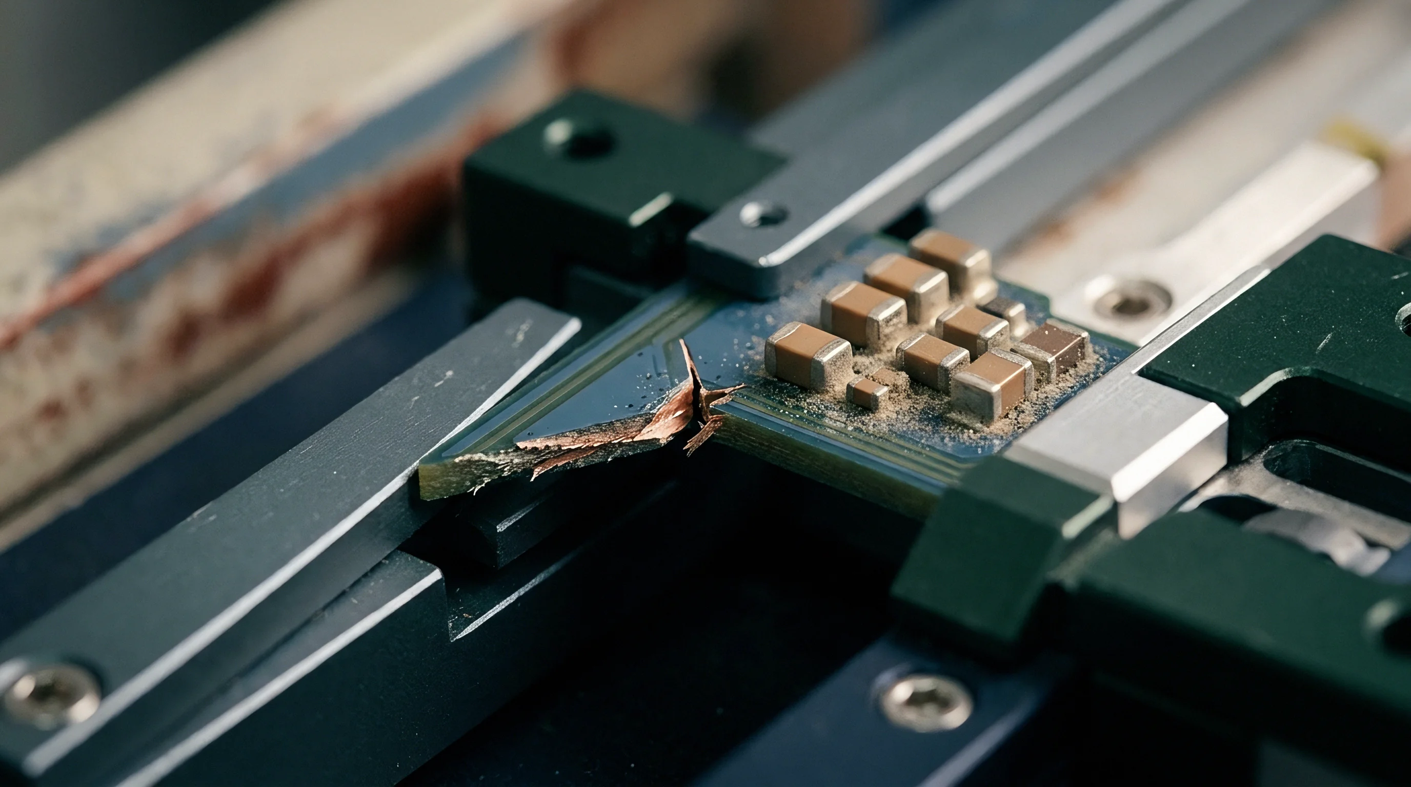
SRAM Wait State Mechanics during Key Generation
Executing elliptic-curve cryptography or symmetric key derivation forces the central processor to fetch continuous instruction streams while fetching large array blocks. Microcontrollers operating at 16 MHz or 32 MHz with reduced supply voltages introduce wait states when accessing internal non-volatile memory or secondary static RAM banks. When flash memory requires two wait states per cycle, instruction prefetch buffers mitigate delays during linear code execution.
Cryptographic loops branching across randomized memory locations break instruction prefetch efficiency. The core stalls on every cache miss, forcing the bus matrix to arbitrate between core instruction fetches and hardware cryptographic accelerator data transfers.
An internal RAM bus contention delay of 45 microseconds at 16 MHz core clock extends AES-128 key generation time by 21 percent under active radio reception.
Hardware security modules offload block cipher calculations from the primary processor core. These accelerators pull key material directly from RAM via system DMA channels. When the core processor simultaneously attempts to write network state updates to internal memory while the cryptoprocessor reads key arrays, bus matrix contention locks execution.
Memory access contention halts the cryptoprocessor pipeline until the central core completes its write stroke. This internal hardware blocking converts what should be a 1.2-millisecond cryptographic operation into a 3.5-millisecond active processing event.
- The node radio receives an encrypted network key rotation frame over the air.
- Central processing hardware triggers an interrupt to suspend low-power sleep state timers.
- System clocks scale from 32 kHz sleep frequency to 32 MHz active core speed.
- Direct Memory Access transfers incoming payload bytes from the radio FIFO to volatile RAM buffers.
- Hardware cryptographic engines pull key material while triggering bus arbitration locks against core instruction fetches.
- Updated key derivatives write to non-volatile flash memory, triggering erase wait states across the internal bus matrix.
Sustained wait states during cryptoprocessor memory fetches drive battery drain beyond the energy allocated for annual maintenance cycles.


Jitter
Variations in processing speed during cryptographic updates directly alter the power profile of battery-operated microcontrollers. Coin cells exhibit high internal resistance. Voltage droop triggers system reset thresholds.
When memory execution delays hold an MCU in active mode during cryptographic processing, total milliampere-second energy consumption scales linearly with the added clock cycles. Cryptographic calculations consume significant peak current. Simultaneously running the radio receiver and internal memory programming circuits creates severe current spikes on the power delivery network.

Current Profiling and Supply Voltage Droop
Active current consumption rises sharply when cryptoprocessor blocks engage alongside receiver circuits. On a standard CR2032 lithium primary coin cell, an active current draw of 15 milliamperes causes an immediate voltage drop due to the internal equivalent series resistance of 10 to 30 ohms. If memory wait states extend the active execution window from two milliseconds to ten milliseconds, the sustained load pulls cell terminal voltage below the microcontroller brown-out reset voltage of 1.8 volts.
Memory wait states extend execution time. A brown-out event during key rotation corrupts security state tables, leaving the mesh node isolated from the network.
| Memory Architecture | Wait States | Execution Time (ms) | Peak Current (mA) | Battery Voltage Droop (mV) |
|---|---|---|---|---|
| Zero-Wait SRAM | 0 | 1.42 | 8.1 | 42 |
| Cached Flash (64 KB) | 2 | 2.88 | 9.4 | 88 |
| Uncached Flash | 4 | 5.12 | 11.2 | 145 |
| External QSPI PSRAM | 8 | 9.65 | 14.8 | 230 |
Integrated power management units attempt to compensate for supply drops by increasing switching regulator duty cycles. System clock speed alters latency penalties. When the internal memory bus stalls, peripheral clock trees remain fully driven despite zero instruction throughput.
Logic analyzers capture exact current profiles. The current integral across the re-keying sequence increases, consuming power budget originally reserved for thousands of idle mesh keep-alive heartbeats.
Decoupling cryptographic payload expansion from non-volatile write routines prevents battery voltage dropouts during mesh key updates.
Silicon vendors frequently attribute key rotation delays to user software inefficiently managing non-volatile flash page clearing.

Spike
Transmitter active durations extend when data access delays hold up outgoing packet assembly. Low-power mesh protocols operate on tight time synchronization. Retransmissions multiply network power consumption.
Radio receivers drop incoming mesh frames. When a node processes a multi-hop group re-keying message, it must acknowledge receipt within a specified Medium Access Control layer window. Bus stalls occurring while decrypting incoming security parameters delay MAC acknowledgment packet construction, forcing the transmitting parent node to assume frame loss and initiate retry mechanisms.

Why Do Memory Bus Stalls Drop Mesh Acknowledgments?
Radio peripherals operating under precise time-division schedules require immediate payload access to construct outgoing acknowledgment frames within strict protocol windows. If the central processor cannot fetch the key confirmation material from flash memory due to flash erase or write wait states, the radio hardware buffer remains empty when the acknowledgment transmission window opens. The physical layer transmits an empty or truncated frame, or misses the transmit slot entirely.
Neighboring nodes record a packet drop, increasing local link contention as retry algorithms trigger across the local RF channel.
| Flash Erase Latency (ms) | MAC Ack Timeout (ms) | Packet Loss Rate (%) | Mean Retransmissions | Network Re-Keying Time (s) |
|---|---|---|---|---|
| 0 (RAM Buffer) | 10 | 0.4 | 1.02 | 4.1 |
| 15 (Page Write) | 10 | 3.8 | 1.18 | 5.8 |
| 45 (Sector Erase) | 10 | 18.2 | 1.85 | 14.2 |
| 120 (Mass Erase Stall) | 10 | 46.5 | 3.40 | 38.9 |
Cascading retransmissions stall the entire mesh network during security updates. Non-volatile writes lock the core bus. Nodes queued to receive updated network keys spend extra airtime listening on congested channels while holding high-power active receiver states.
In dense deployments of three hundred nodes or more, latency spikes during key propagation create RF channel saturation, dropping legitimate sensor traffic and forcing repetitive, energy-intensive network joins.
Compliance with Bluetooth Mesh profile version 1.1 requires key refresh procedures to complete without invalidating active replay protection caches.
Keeping encryption keys in high-speed zero-wait-state RAM prevents radio receiver buffer overflows during multi-hop group update broadcasts.


Vault
Partitioning volatile memory structures prevents processor blocking during cryptographic key rotation cycles. Double buffering eliminates memory bus contention. Direct memory access reduces active airtime.
System architects split incoming packet buffers into dedicated SRAM banks that operate completely isolated from core execution structures. By assigning the radio DMA controller exclusive access to RAM Bank 0 while the core processor executes key derivation algorithms out of RAM Bank 1, hardware contention vanishes from the internal bus matrix.

Non-Volatile Decoupling and Flash Allocation
Writing updated security credentials to internal flash memory involves physics that halt system bus access for several milliseconds. Single-bank flash microcontrollers enforce a complete core stall during flash page write or sector erase operations. To maintain mesh timing, firmware architectures store updated network keys in RAM temporary buffers, delaying non-volatile commit routines until radio peripheral activity ceases entirely.
Consider an operational timing window during a network-wide re-keying campaign. A node receives an 80-byte re-key packet at 0 dBm transmit power, consuming 12 milliamperes for 2.56 milliseconds during RF reception. Processing the payload AES-128-CCM key derivation in zero-wait-state SRAM requires 1.10 milliseconds at 8 milliamperes core current.
Writing the derived key directly to internal flash during active reception stalls the bus for 15 milliseconds at 14 milliamperes peak current. Deferring the flash write until the radio closes its acknowledgment window saves 185 microcoulombs of charge per re-keying event, preserving battery operational lifespan.
- Zero-Copy Buffering allocates contiguous volatile memory spaces for incoming network frames to prevent core memory relocation overhead.
- Deferred Flash Commit holds updated key blocks in volatile RAM structures until radio peripherals return to sleep mode.
- Dual-Bank Instruction Prefetch routes cryptographic execution through cached RAM structures while non-volatile storage controllers execute sector erases.
- Priority Bus Arbitration assigns high priority to radio DMA requests over core instruction fetches during active packet reception windows.
Firmware structures managing volatile key storage enforce operational rules to prevent timing failures during security updates.
- Static Buffer Allocation prevents heap fragmentation and runtime allocation delays during emergency key revocation sequences.
- RAM Execution Execution Routing places time-critical security routines inside zero-wait-state SRAM instruction memory.
- Interrupt Masking Isolation prevents background timer interrupts from interrupting atomic key generation loops.
- Voltage Monitor Interlocks suspend non-volatile flash commit routines if coin cell terminal voltage dips below safe operational thresholds.
The IEEE 802.15.4 specification mandates frame security processing times that force hardware designers to isolate flash write operations from MAC layer acknowledgment timers.


Margin
Bench validation of low-power node firmware isolates execution delays through direct current probes and logic analysis. Bench testing reveals unoptimized flash access. Engineers monitor supply lines using current profiling hardware capable of microsecond sampling rates alongside digital logic analyzers tracking memory bus control pins.
Precise power profiling reveals hidden instruction stalls, cache misses, and flash write holds during real-time mesh security updates.

Bench Measurement Techniques for Bus Wait Latency
Hardware probes attached to memory bus control lines allow engineers to observe cycle-accurate execution stalls during key updates. Toggling general-purpose input-output pins at the start and end of cryptographic functions provides accurate execution duration measurements on an oscilloscope screen. Coupling these digital signals with shunt resistor current traces correlates memory wait states directly to supply power peaks.
If an MCU remains in high-current active modes longer than predicted by raw instruction cycle counts, memory bus contention or flash wait states account for the discrepancy.
Quantifying latency impacts requires rigorous test suites executing re-keying operations under varied channel conditions and battery depletion stages. Test benches simulate weak link budgets by introducing attenuators into the RF path, forcing the system to evaluate key processing efficiency during high packet loss scenarios. Software tools inject simulated RAM bus congestion by running concurrent background DMA transfers during key generation cycles.
Isolating memory subsystem performance from raw RF performance prevents misdiagnosing firmware processing stalls as simple wireless path loss.
Whether lower clock frequencies with zero wait states outperform overclocked cores with frequent cache misses during dense mesh re-keying remains an open question for battery-powered nodes.