Integrated Circuit Lithography Shrink Impact on Interface Signal Integrity
Advanced lithography shrinks lower interface supply voltages and compress driver swing, requiring strict package channel extraction to prevent signal eye closure.
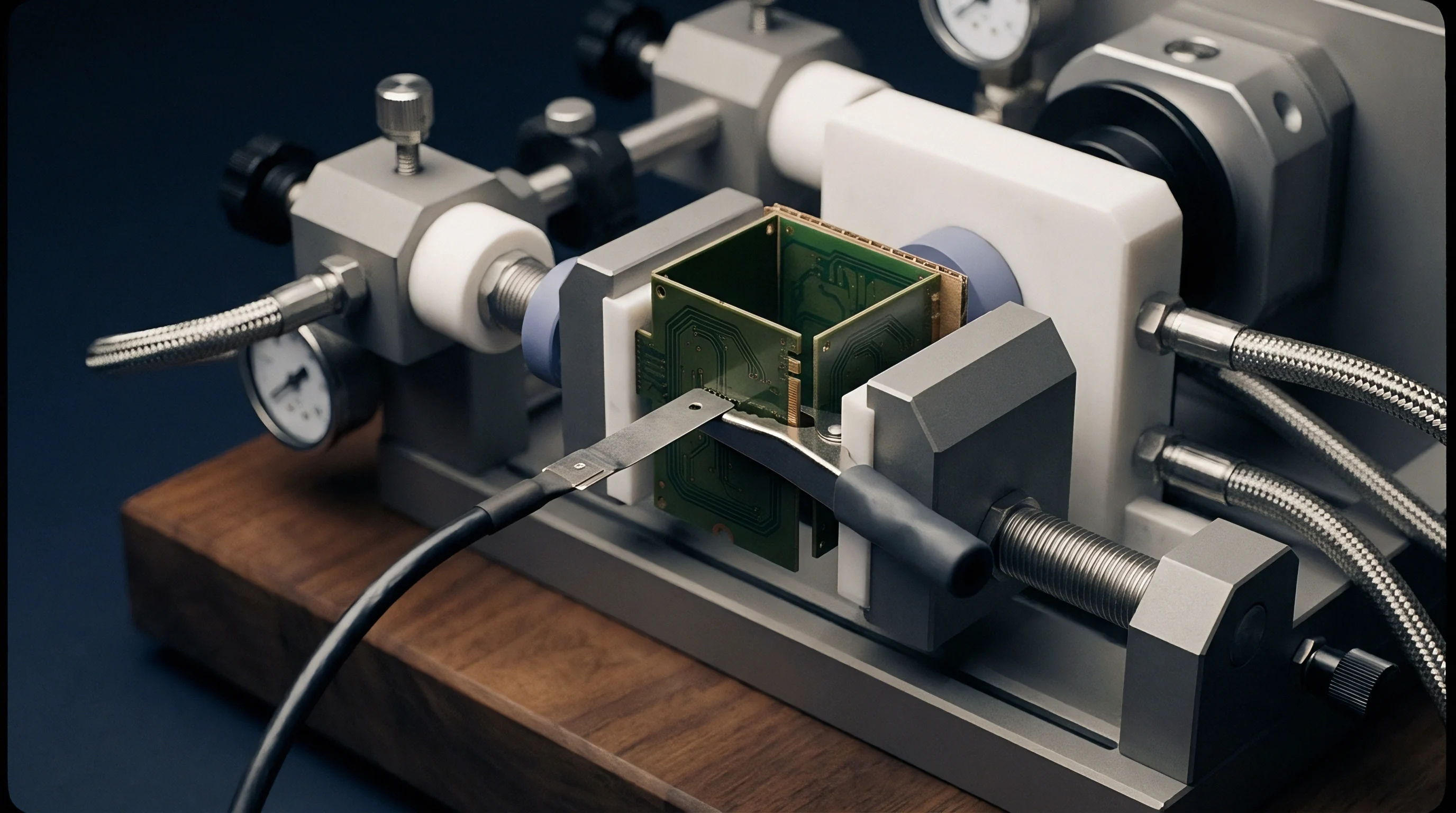

Die
Deep submicron lithography scaling reduces physical gate lengths and supply voltage rails while forcing interface input-output circuits into tighter physical envelopes. Downward voltage scaling from 1.2V in legacy planar nodes to 0.75V and below in advanced FinFET and Gate-All-Around architectures diminishes signal amplitude at the silicon pad. Reduced voltage swing directly lowers the signal-to-noise ratio of physical layer transceivers before high-speed channels add transmission losses.
The physical gate oxide shrinks to atomic dimensions, increasing subthreshold leakage currents and thermal dissipation density within high-speed input-output driver banks.
Transistor threshold voltage variations increase relative to nominal operating voltages as silicon lithography advances past the 7nm node. Microscopic dopant fluctuations and edge roughness in fin profiles create drive current mismatches across parallel driver slices. Driver impedance varies across manufacturing process corners, altering transmitter source termination accuracy and triggering unwanted channel reflections.
Interface designs using multi-level signaling schemes like PAM4 suffer severe eye degradation when driver linearity fluctuates across supply noise spikes.
Dynamic supply voltage drop exceeding five percent of nominal rail reduces transmitter output slew rates by up to twelve percent in sub-5nm interfaces.
Lower operating voltages reduce driver headroom, compressing the linear operating region of analog front-end circuits. Dynamic voltage drops on power supply networks modulate the driver edge rate, transforming power rail noise directly into transmitter duty-cycle distortion and deterministic jitter. On-chip power distribution networks face higher current densities, causing localized phase noise in phase-locked loops responsible for clock generation.
Micro-bump layouts on die pads become dense as pin counts scale upward within micro-scale bump pitches. On-chip metal interconnect layers suffer from elevated parasitic resistance as conductor cross-sections narrow. Narrower metal traces elevate self-heating effects and electromigration risks while increasing mutual inductive and capacitive cross-coupling between adjacent transmitter lanes inside the die shadow.

Silicon Scaling Parameters
Physical parameters change rapidly as transceivers move from planar geometries to advanced multi-gate nodes. The operational trade-offs impact interface noise floor levels, edge speed, and termination accuracy.
| Process Node | Nominal VDD | Transmitter Swing | Pad Bump Pitch | Random Jitter Floor |
|---|---|---|---|---|
| 28nm Planar | 1.20 V | 800 mV p-p | 150 um | 250 fs RMS |
| 16nm FinFET | 0.85 V | 600 mV p-p | 110 um | 180 fs RMS |
| 5nm FinFET | 0.75 V | 500 mV p-p | 55 um | 120 fs RMS |
| 3nm GAAFET | 0.65 V | 400 mV p-p | 40 um | 95 fs RMS |
Edge rates accelerate as intrinsic transistor switching delays decline in smaller nodes. Fast rise and fall times under 15 picoseconds excite high-frequency parasitic modes within the die-package transition structure. Discontinuities that were electrically invisible at lower switching rates now act as prominent impedance mismatches, sending energy reflecting back into the silicon transmitter output stages.
Failure to align driver supply bounds with package resonance frequencies destroys channel margins before signals reach the bump.

Channel
High-speed interface signals leaving the chip die must pass through micro-bumps, redistribution layers, package substrates, socket contacts, and printed circuit board traces. Interconnect paths face severe frequency-dependent attenuation at high data rates. Advanced silicon lithography allows chip interfaces to operate at 32, 64, and 128 Gigabits per second per lane, but high-frequency signal energy dissipates rapidly into dielectric substrate materials.
Skin effect resistive losses expand as signal frequency increases, restricting current flow to the ultra-thin outer boundaries of copper trace conductors. Surface roughness on package and circuit board copper foil magnifies this resistive attenuation by forcing current along a longer effective path length. Dielectric absorption dissipates energy directly into the epoxy resin matrices of printed circuit substrates, collapsing signal amplitude prior to receiver sampling.
Inter-symbol interference dominates interface channel degradation at gigabaud symbol rates. High-frequency signal components arrive attenuated relative to lower-frequency patterns, spreading symbol energy across adjacent unit intervals and closing the signal eye horizontally and vertically. Impedance discontinuities at via transitions, micro-bump pads, and connector interfaces reflect energy into the channel, generating complex standing waves that interfere with incoming data patterns.
- Via Stub Discontinuity generates acute resonance notches in channel insertion loss responses when stub lengths exceed one-tenth of the signal wavelength.
- Glass Weave Skew induces differential phase mismatch when differential trace pairs cross alternating resin-rich and glass-fiber-dense substrate zones.
- Crosstalk Coupling transfers high-frequency noise between densely spaced traces through fringing electric and magnetic fields within package layers.
- Mode Conversion converts differential signal energy into common-mode noise when trace physical asymmetries emerge along high-density routing paths.
High routing density around fine-pitch silicon package bumps forces trace lines into close physical proximity. Electric and magnetic field coupling creates forward and backward crosstalk between adjacent physical channels. Dense micro-via arrays in high-density interconnect substrates introduce local ground return path breaks, forcing high-frequency return currents onto longer routes and elevating common-mode noise levels.
Standard IPC-2152 temperature limits constrain current-carrying trace dimensions, forcing high-density interface routing into high-loss substrate configurations.
Die-to-die interfaces inside multi-chip modules rely on silicon interposers or organic redistribution layers. While trace lengths remain short inside advanced packages, parasitic capacitance at fine-pitch micro-bumps combines with interposer trace inductance to create tight LC resonance peaks. These package-level parasitics alter the phase response of the channel, eroding differential timing margins.
High speed traces layout integrity improves when ground return vias mirror signal via transitions directly on adjacent grids.


Model
Accurate behavioral representations of transceiver architecture are required to predict high-speed signal transmission behavior over real lossy channels. Legacy analog SPICE models fail to simulate millions of operational unit intervals efficiently due to long computation times. Algorithmic Modeling Interface formats split high-speed transceiver representations into analog buffer characteristics and executable algorithmic code, enabling fast statistical and time-domain signal processing simulations.
Lithography shrinks introduce complex non-linear driver behaviors that simple behavioral models fail to capture. Sub-5nm physical layer transceivers incorporate adaptive Continuous-Time Linear Equalization and multi-tap Decision Feedback Equalization directly inside the analog front end. Executable code blocks must represent dynamic digital adaptation algorithms accurately, including finite coefficient resolution, internal quantization noise, and tap saturation limits under real silicon operating conditions.

Behavioral Representation Quality
S-parameter models describing passive channels, package substrates, and micro-bump transitions must adhere to physical laws before incorporation into high-speed interface simulation environments.
- Causality Enforcement eliminates non-physical precursor responses where output energy appears prior to signal input excitation during time-domain impulse transformations.
- Passivity Checking ensures that passive multi-port network models do not generate artificial energy across all evaluated frequency sweep points.
- Reciprocity Verification guarantees balanced transfer matrices between symmetric port pairs across the evaluated frequency spectrum.
- DC Extrapolation Integrity provides stable low-frequency boundary values down to zero Hertz to maintain baseline wander accuracy in time-domain runs.
Port termination choices during electromagnetic field extraction determine S-parameter validity. Truncating frequency sweeps too early introduces truncation artifacts during inverse fast Fourier transforms, creating artificial ringing in time-domain eye diagrams. Power-aware IBIS models must account for simultaneously switching noise by linking driver buffer models directly to on-die and package power delivery network impedance profiles.
| Parameter | Model Assumption | Silicon Reality | Eye Margin Impact |
|---|---|---|---|
| Driver Impedance | Ideal 50 Ohm nominal | Non-linear voltage dependent | 2.5 dB return loss drop |
| DFE Tap Adaptation | Infinite precision floats | 5-bit to 7-bit quantized integers | 12 percent height error |
| CTLE Peaking Gain | Continuous linear steps | Discretized control steps | 0.08 UI jitter variation |
| PDN Noise Injection | Static VDD rail | High-frequency voltage ripple | 15 percent width reduction |
Discrepancies between simulated behavioral models and physical silicon arise when packaging parasitics are mischaracterized or simplified. Transceiver vendors attribute eye diagram discrepancies to unmodeled printed circuit board manufacturing tolerances rather than behavioral driver flaws.


Margin
Physical bring-up verification of advanced interface silicon requires precise bench instrumentation and repeatable measurement procedures. Bit error rate targets of 10 to the power of negative 12 for PCIe or 10 to the power of negative 15 for memory buses demand automated test routines capable of sweeping voltage and phase offsets simultaneously. Real-time oscilloscopes capturing signals above 30 Gigahertz require high-bandwidth active probes that minimize capacitive loading on fine-pitch circuit board test points.

How Does Equalization Recover Lost Eye Margin?
Receiver continuous-time linear equalization boosts high-frequency spectral components relative to low-frequency energy to compensate for channel insertion loss. Multi-tap decision feedback equalization then adds weighted delayed decisions to the analog input, subtracting inter-symbol interference caused by reflections and dispersion. Integrated equalization logic opens completely closed real-world signal eyes at the internal sampler plane, restoring timing and amplitude margins inside the receiving silicon.
- Connect low-loss phase-stable coaxial cables between the evaluation board package test points and the high-bandwidth oscilloscope input channels.
- Load the nominal silicon register settings for physical layer transmitter output amplitude, pre-cursor deemphasis, and post-cursor deemphasis taps.
- Perform frequency-domain S-parameter calibration on the measurement cables and fixture adapters to de-embed test point parasitics from raw waveforms.
- Run receiver jitter tolerance testing by injecting controlled random jitter and sinusoidal jitter profiles using a high-speed bit error rate tester.
- Sweep receiver internal decision feedback equalization tap coefficients while monitoring internal signal eye height and width registers using vendor-specific diagnostic software.
Oscilloscope noise floors, clock jitter, and cable losses erode measured timing margins during high-speed physical testing. Receiver eye margin measurements conducted at internal sampler pads must rely on built-in on-die oscilloscope diagnostic circuits, as physical probes cannot access silicon bumps directly without altering channel impedance.
Built-in self-test hardware registers provide direct access to internal receiver signal eye dimensions after equalization algorithms settle.
Voltage and temperature corner testing exposes operational instability across physical silicon variations. Thermal expansion changes dielectric properties, altering trace propagation velocity and channel loss characteristics over extended operational periods. Whether die-level thermal aging introduces deterministic jitter drift across extended field deployments remains a subject of ongoing laboratory qualification.

Charge
Architectural lithography decisions carry high financial stakes during physical layer silicon IP integration. Moving an interface PHY design to an advanced process node demands non-recurring engineering expenditure that must be weighed against system performance goals. A single mask set re-spin at sub-5nm nodes can cost upwards of fifteen million dollars, making signal integrity validation a critical gating factor in project financial models.
Semi-custom integration allows buyers to license proven silicon transceiver physical layer designs while tailoring package substrate routing and channel interconnect configurations. Turnkey integration transfers physical implementation scope to external design houses, shifting layout and verification liability. Clear demarcation lines in design transfer documentation determine which engineering entity bears the cost of non-pass signal integrity compliance checks during silicon bring-up.
| Engineering Scope Item | Turnkey Integration | Semi-Custom PHY | White-Label Silicon |
|---|---|---|---|
| PHY IP Licensing Fee | Bundled in NRE | Direct License Fee | Silicon Unit Price |
| Package SI Verification | Integrator Owned | Shared Ownership | Buyer Owned |
| IBIS-AMI Model Delivery | Included in Package | IP Vendor Standard | Generic Reference Only |
| Silicon Respin Liability | Integrator Warranted | Conditional IP Warranty | Buyer Assumed Risk |
Scope contracts must explicitly state physical deliverable requirements, including raw 3D full-wave electromagnetic simulation files, package GDSII routing databases, and correlated S-parameters. Unclear acceptance test definitions leave buyers vulnerable to integration delays when physical transceivers fail channel compliance benchmarks due to unmodeled package-to-board discontinuities.
Non-recurring engineering quotes that omit full channel signal integrity modeling across extreme manufacturing corners create budget overruns late in the product development cycle. Silicon vendors frequently bound physical layer compliance to idealized evaluation board channels, leaving system integrators responsible for custom substrate loss mitigation. A standard silicon acceptance addendum assigning high-speed interface compliance failure liability directly to the layout integrator shifts re-spin expense onto the system builder.