Managing Dynamic Contact Resistance Drift in High Current Automated Test Fixtures under Continuous Thermal Load
Manage dynamic contact resistance drift by isolating sense lines with four-wire Kelvin probes and active cooling to prevent electrothermal asperity creep.
Constriction
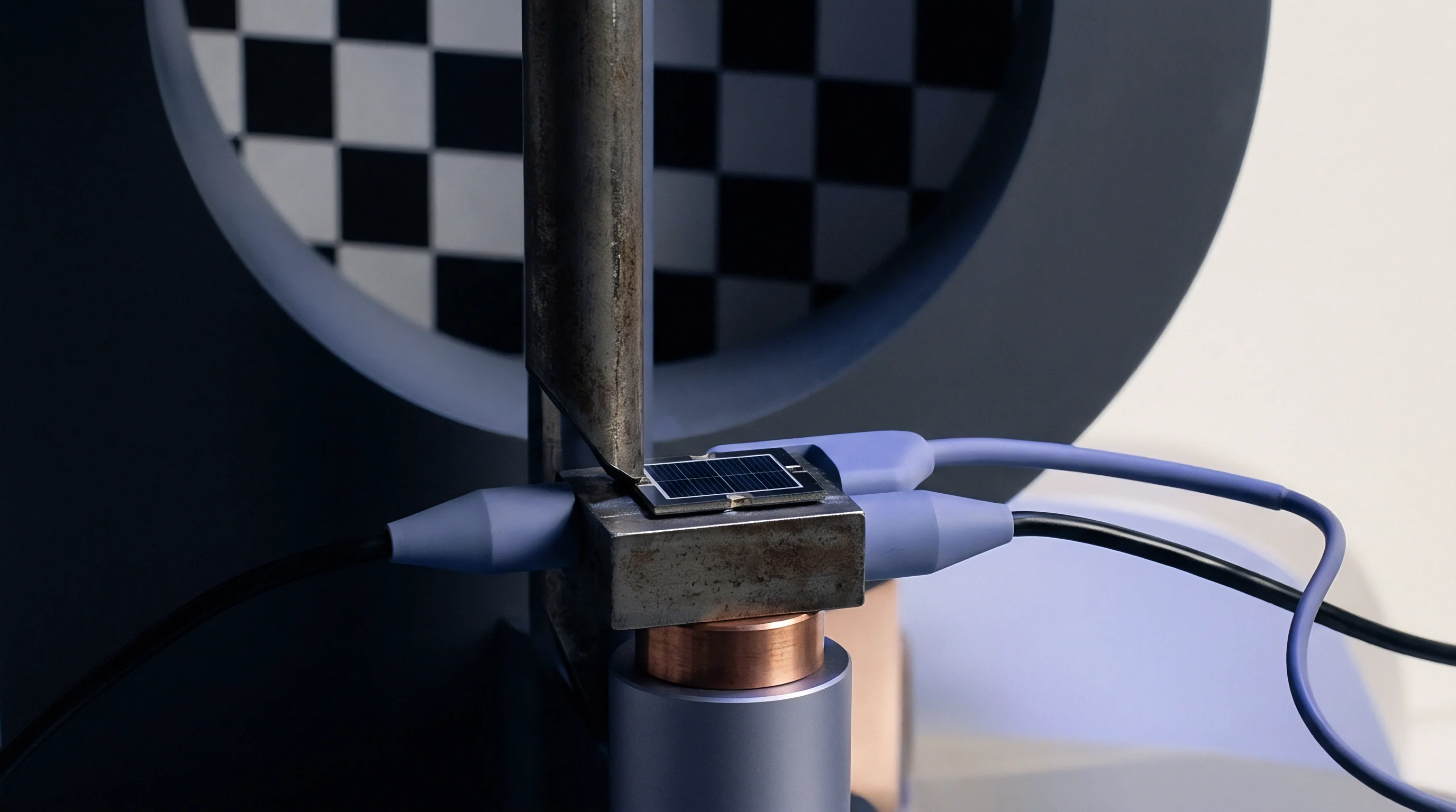
Current forced through a physical contact interface concentrates into microscopic junction spots termed a-spots. The true metallic contact area spans less than one percent of the apparent mating area under typical mechanical engagement forces. Total contact resistance splits across the constriction value, governed by Holm constriction mechanics, and film resistance caused by surface oxides, contaminants, and corrosion products.
When test fixtures pass sustained currents between 50 A and 500 A into power electronics modules, battery tab terminals, or power distribution units, localized I-squared-R dissipation generates extreme localized thermal gradients. Peak temperatures at individual a-spots frequently exceed bulk probe temperatures by 40 °C to 90 °C, accelerating chemical kinetic degradation mechanisms at the mating boundary.
Automated high-throughput test environments exacerbate these thermodynamic phenomena through continuous mechanical actuation cycles. Automated test equipment introduces micro-scrubbing actions across consecutive insertions. Thermal expansion mismatches between probe materials, test socket housings, and device under test contact pads induce secondary cyclic micrometer-scale slip.
This relative displacement strips thin passive noble metal coatings, exposing reactive substrate layers to atmospheric oxygen at elevated operational temperatures.
ASTM B539 test methods mandate dry-circuit four-wire Kelvin sensing below twenty millivolts open-circuit potential to measure constriction values without puncturing fragile surface tarnish films.
Electrical engineers witness dynamic resistance drift during continuous load cycles when contact interfaces enter thermal runaway regimes. Elevated a-spot temperatures increase localized metal resistivity via standard temperature coefficients. Higher resistance generates additional heat under constant-current test sequences.
The mechanical yield strength of the contacting asperities drops as localized bulk temperatures approach homologous annealing thresholds. Asperities deform plastically, enlarging the contact patches, while concurrent thermal oxidation grows semi-insulating intermetallic films along the perimeter of each spot. The competition between mechanical creep enlargement and oxidative film growth determines whether measured loop resistance drops momentarily or rises monotonically during a prolonged dwell.
Predicting Electrothermal Asperity Softening
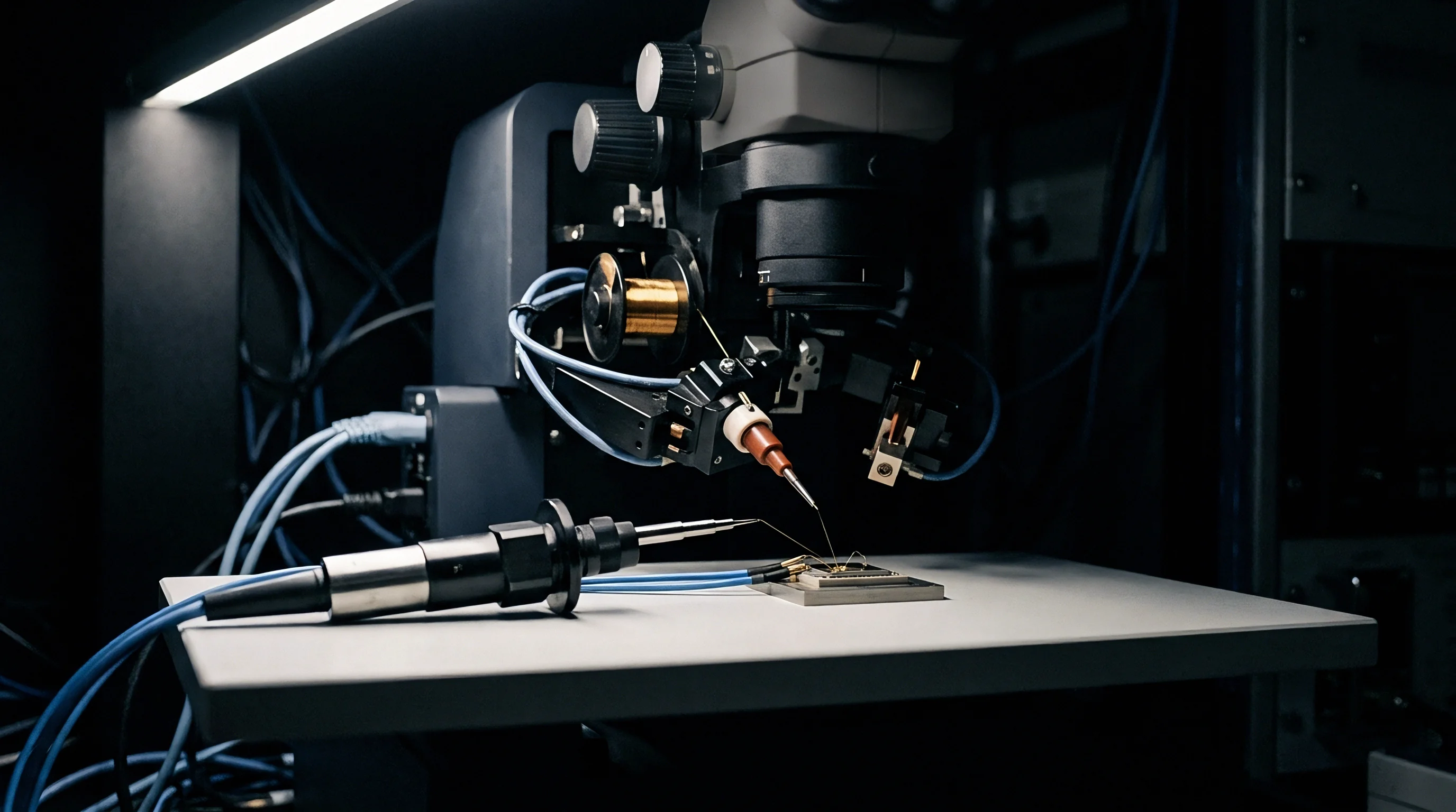
The equilibrium voltage drop across a metallic contact constriction correlates with the maximum internal contact temperature through the Kohlrausch relation. When the potential difference across an individual contact boundary reaches the softening voltage of the metal, asperity crush strength degrades rapidly.
Copper softens near 120 millivolts, corresponding to an internal constriction temperature of approximately 190 °C. Gold interfaces reach softening thresholds at merely 70 to 80 millivolts, representing temperatures near 100 °C. Applying high continuous test currents across worn, oxidized, or under-clamped test pins pushes localized contact drop beyond these critical potentials. The pin tip yields mechanically, increasing the true metallic mating area. This mechanical flattening temporarily lowers electrical resistance.
Subsequent exposure to elevated ambient air oxidizes the newly exposed copper or nickel base metal, forming high-resistance cuprous oxides and nickel oxides. The next insertion cycle exhibits severe contact resistance variability, distorting precision voltage and efficiency measurements on the production line.
False failures multiply across automotive inverter and battery cell testing lines when this electrothermal instability remains uncompensated. Test engineers frequently replace device modules under test, misdiagnosing probe degradation as defective component terminal bonding.

Metallurgy
Selecting appropriate alloys, sub-layers, and surface finishes determines the baseline operational lifespan of high-current test contacts. Beryllium copper and tellurium copper serve as standard substrate conductors for pogo pins, stamped fingers, and spring-loaded crown tips. Beryllium copper alloy C17200 provides tensile strength exceeding 1100 megapascals in the TH04 temper, retaining mechanical compliance across thousands of actuations.
Tellurium copper alloy C14500 offers superior bulk electrical conductivity at 93 percent International Annealed Copper Standard, lowering body resistive heating under 100 A sustained continuous loads.
Plating stacks protect base copper alloys against oxidative fouling. Standard commercial probe pins feature an electrolytic nickel barrier layer coated with hard cobalt-gold or palladium-nickel alloys. Gold exhibits excellent chemical nobility and zero native oxide formation under standard ambient atmospheric storage.
Cobalt additions harden electroplated gold to 130 to 200 Knoop hardness units, enhancing abrasive wear endurance. Gold atoms diffuse outward through micro-porosities in thin barrier layers when subjected to continuous interface temperatures above 125 °C. Nickel migrates to the outer surface, forming hard dielectric nickel oxide crusts within dozens of operational hours.
| Plating Stack Composition | Microhardness (HV) | Maximum Operating Temperature (°C) | Fretting Wear Resistance | Bulk Resistivity (μΩ·cm) |
|---|---|---|---|---|
| Hard Gold (0.75 μm Au-Co over 2.5 μm Ni) | 140 to 200 | 125 | Moderate | 2.4 |
| Palladium-Cobalt (1.0 μm Pd-Co over Ni) | 350 to 450 | 200 | High | 10.8 |
| Rhodium Flash (0.5 μm Rh over 3.0 μm Ni) | 700 to 800 | 300 | Very High | 4.5 |
| Silver-Nickel Alloy (5.0 μm Ag over Cu) | 90 to 130 | 180 | Low | 1.6 |
Silver finishes deliver exceptionally low contact resistance and maximum thermal conductivity. Silver remains susceptible to ambient sulfur tarnishing, creating silver sulfide films. Under high electrical stress, silver atoms undergo rapid electromigration along grain boundaries, especially in the presence of continuous direct current and thermal gradients exceeding 10 °C per millimeter.
Will Thermal Cycling Accelerate Asperity Creep?
Thermal excursions induce mechanical relaxation in spring-loaded probe assemblies. Springs fabricated from music wire or standard stainless steel grades lose initial pre-load force rapidly when held at temperatures above 100 °C. Precipitation-hardened beryllium copper and specialized high-nickel superalloys such as Inconel X-750 resist spring relaxation up to 250 °C. The loss of clamping force shrinks the real contact area proportionally, driving constriction resistance upward through the test shift.
Intermetallic compound growth introduces brittle, high-resistivity phases at the boundary layer. When testing tin-plated or solder-dipped component leads, molten or solid-state tin transfers onto probe tips. Tin diffuses into gold and copper, yielding intermetallic species such as Cu6Sn5 and AuSn4.
These intermetallic phases feature electrical resistivities four to ten times higher than the pure parent metals. Intermetallic compounds crack under repeated mechanical cyclic shock, producing particulate debris that collects inside pin crowns, creating intermittent open circuits.
Plating specifications for continuous high-current fixtures demand rigorous diffusion barrier engineering. Specifying a dense, low-stress sulfamate nickel barrier layer with a minimum thickness of 3.0 to 5.0 micrometers suppresses thermal substrate out-diffusion. Palladium-nickel intermediate layers capped with a flash of hard gold mitigate noble metal wear-through, extending contact tip operating lifetime to more than 100,000 actuations at 150 °C continuous fixture temperatures.
Periodic chemical analysis of probe tips running automated battery pack end-of-line verification reveals significant substrate contamination after 20,000 cycles if barrier thicknesses fall below 2.0 micrometers.
Stroke
Mechanical engagement dynamics dictate the stability of electrical interfaces. Probe stroke travel, tip geometry, and actuation velocity determine the initial contact area and the extent of surface wipe. Crown-point, chisel-point, and serrated serration geometries concentrate vertical engagement force onto sharp features designed to puncture native oxide sheets.
Flat or hemispherical radiused tips distribute mechanical force across wider footprints, reducing terminal marring while demanding pristine contact surfaces to achieve acceptable resistance values.
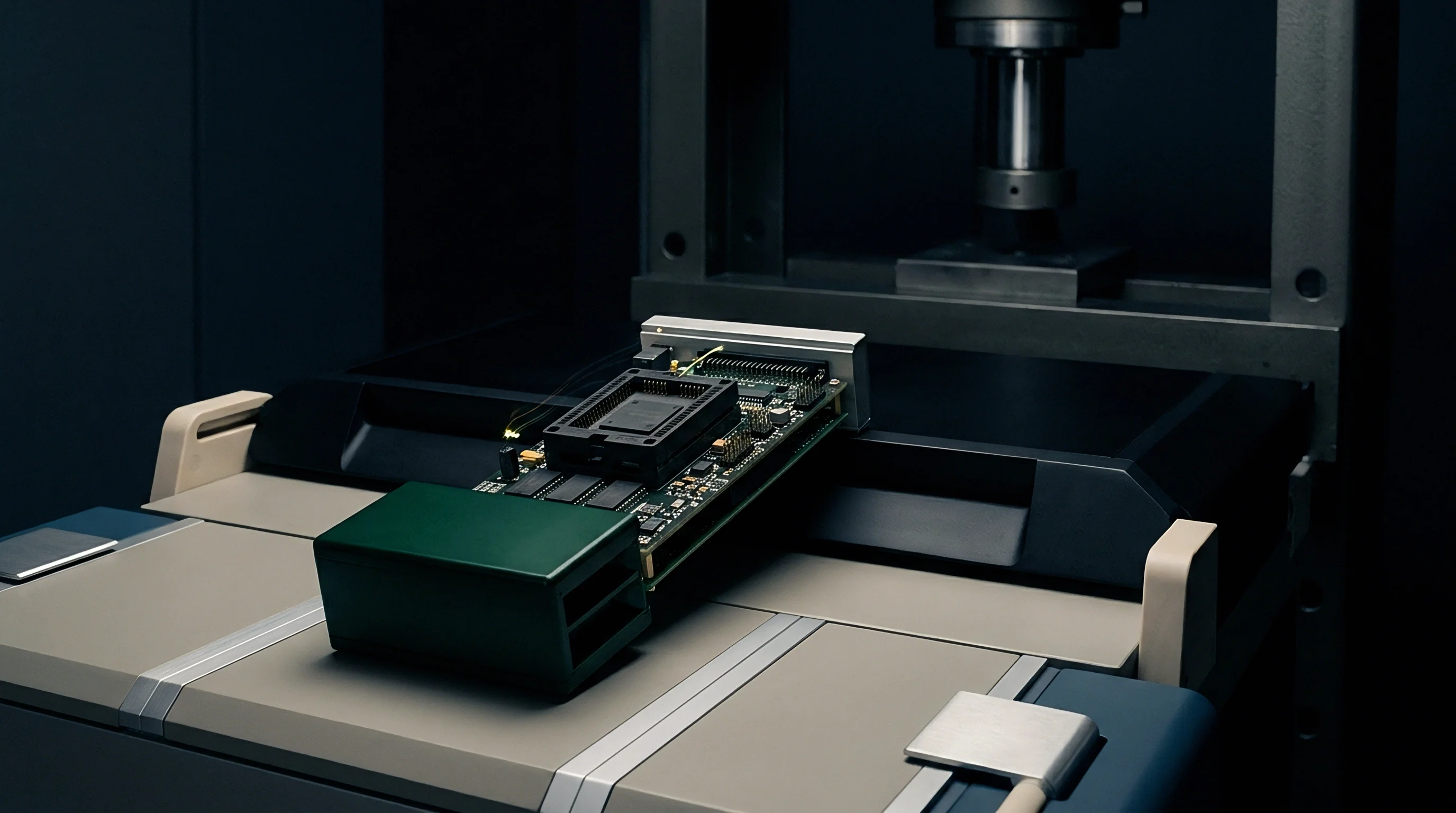
Automated test fixtures rely on pneumatic cylinders, servo presses, or mechanical cams to drive test heads into the device under test. Actuation speed influences probe tip mechanics. Rapid downward velocities cause contact bounce, igniting microscopic electrical arcs when fixtures close under live voltage or residual capacitance.
Arcing pits the mating surfaces, depositing non-conductive vaporized dielectric slag.
A probe tip losing twenty percent of its mechanical pre-load generates a proportional rise in constriction resistance that no software calibration algorithm can decouple from device degradation.
Micro-wiping actions accompany vertical probe compression in high-performance test sockets. Angled plunger shafts or torsion mechanisms translate vertical downward motion into 20 to 100 micrometers of lateral scrub. This controlled sliding scrubs away surface oxidation, dislodges airborne dust particles, and exposes clean underlying metal grains.
Excessive scrub travel wears through thin protective gold plating within thousands of test cycles, accelerating base metal exposure and catastrophic thermal drift.
- Mechanical pre-travel verification establishes the baseline touchpoint position, ensuring complete stroke engagement across all parallel probe tips regardless of manufacturing height tolerances on device under test terminal pads.
- Controlled compression velocity damping limits probe descent speeds to less than 15 millimeters per second, preventing kinetic rebound and eliminating dynamic contact bounce events that trigger micro-arcing.
- Wipe displacement tracking measures real lateral tip movement using laser triangulation displacement sensors during fixture commissioning to confirm oxide clearing without aggressive plating erosion.
- Continuous clamping force retention monitors mechanical pneumatic load cells embedded behind fixture backing plates, ensuring engagement pressures remain stable throughout extended elevated-temperature dwell steps.
- Controlled retraction deceleration manages mechanical release dynamics, preventing sudden mechanical spring snap-back that degrades internal probe spring seats and dislodges retained particulate contaminants.
Parallel testing layouts multiply mechanical tolerances. When testing battery module interconnects requiring eight to twenty parallel high-current pins per terminal, subtle coplanarity deviations across the array create severe current imbalances. A pin seated 150 micrometers higher than its neighbor absorbs greater initial mechanical force, while the recessed pin maintains lower contact force.
Lower contact force yields higher contact resistance. High-current loads divide unevenly across the array, causing the recessed pin to operate hotter, initiating localized thermal runaway, accelerated oxidation, and premature electrical failure.
Fixture design teams must establish strict coplanarity budgets across probe blocks. Tooling plates require precision machining from dimensionally stable materials such as aluminum tooling plate, brass, or ceramic-filled polyimide composites like Torlon 4203. Fixture deflection under total clamping loads exceeding several kilonewtons introduces center-span bowing, causing differential stroke depths between peripheral and internal contact pins.
Reinforcing test head platens with structural steel stiffener ribs eliminates structural deflection, ensuring uniform stroke compression across large-area high-current arrays.
Shunt
Electrical measurement integrity relies upon Kelvin four-wire topologies. In two-wire setups, probe bulk resistance, lead wire resistance, terminal junction potentials, and contact resistance merge indistinguishably into a single measured value. Supplying 100 A through a two-wire connection with a 500-microhm total contact and lead resistance creates a 50-millivolt parasitic offset and generates 5 watts of continuous heat directly inside the measurement path.
True four-wire Kelvin connections segregate the high-current excitation loop from the high-impedance voltage sense loop.
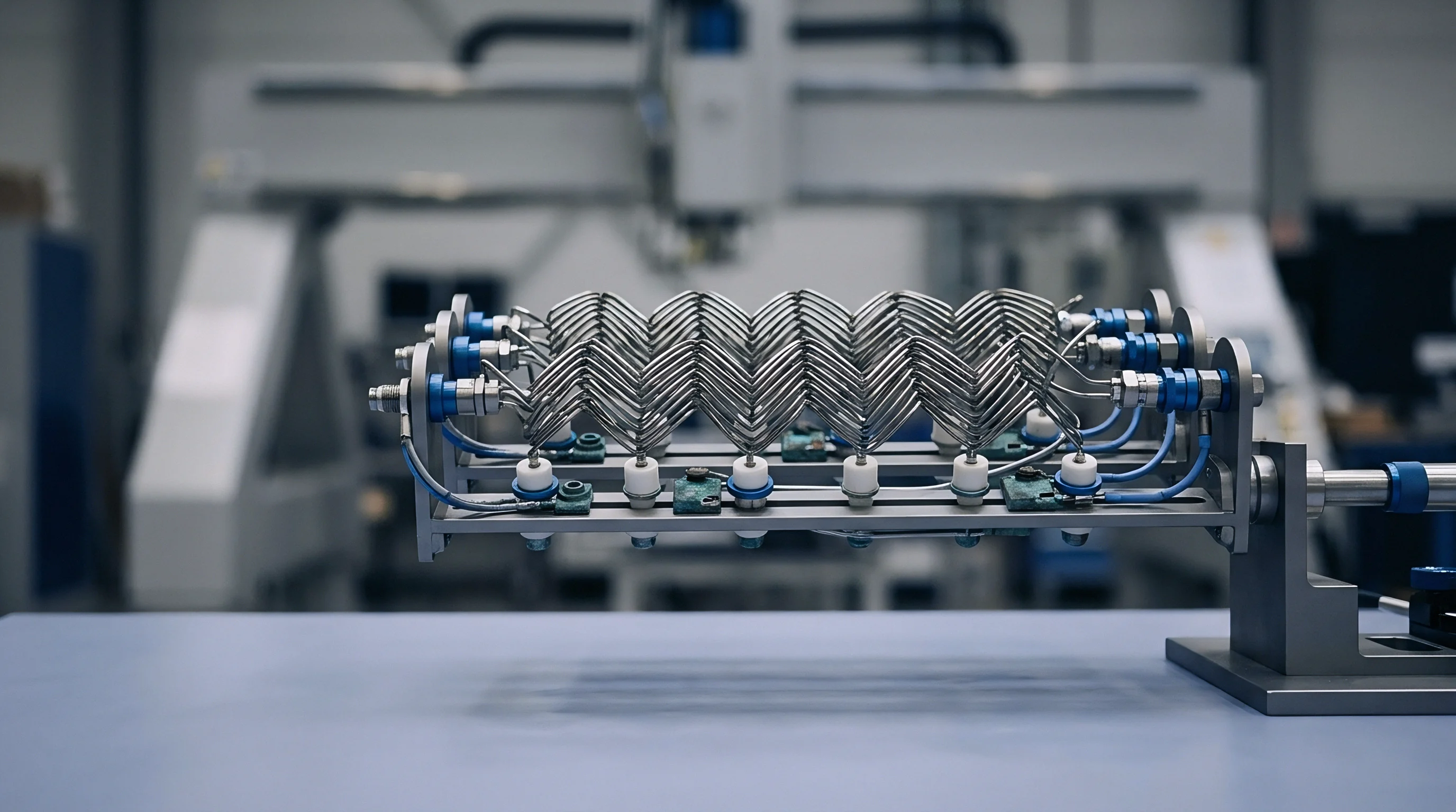
Coaxial high-current Kelvin probes pack both paths into a single mechanical barrel. The outer cylindrical barrel carries continuous drive currents up to 100 A, while an electrically isolated central pogo pin touches the component terminal directly to sample the voltage drop. The inner sense pin draws picoamperes into high-input-impedance digital multimeters, rendering contact resistance drift on the sense pin electrically irrelevant to measurement accuracy.
Contact resistance drift on the high-current outer barrel remains critical. Resistive drift in the current-carrying sleeve generates intense thermal energy that conducts directly into the central sense probe, creating parasitic thermal electromotive force errors across dissimilar metal junctions.
| Contact Junction Metallurgy | Seebeck Coefficient (μV/°C) | Thermal Gradient Across Joint (°C) | Parasitic Offset Voltage (μV) | Induced Measurement Error at 10 mV Full Scale (%) |
|---|---|---|---|---|
| Copper to Beryllium Copper | 1.5 | 35 | 52.5 | 0.525 |
| Copper to Gold Plated Nickel | 3.0 | 45 | 135.0 | 1.350 |
| Copper to Constantan Reference | 40.0 | 20 | 800.0 | 8.000 |
| Tellurium Copper to Copper | 0.2 | 25 | 5.0 | 0.050 |
Thermoelectric voltages arise whenever thermal gradients span junctions between dissimilar conductive metals. Seebeck coefficients dictate the magnitude of the parasitic voltage generated per degree Celsius of temperature differential. When an outer drive sleeve runs at 140 °C while the inner sense tip sits at 95 °C, thermal diffusion through the air gap or internal polyimide insulating sleeves creates significant thermal disparities.
The resulting microvolt-level Seebeck offsets distort sub-milliohm direct-current resistance measurements, misleading battery internal resistance calculations and power MOSFET on-resistance qualifications.

Do Voltage Drops Mask False Rejections?
Parasitic voltage offsets shift digital multimeter readings unpredictably. In high-volume manufacturing lines, component binning software tests devices against tight sub-milliohm tolerance windows. A parasitic Seebeck offset of 100 microvolts under a 10 A test current equates to a 10-microhm apparent resistance error.
When measuring power busbars specified at 50 microhms with a plus-or-minus five percent pass boundary, a 10-microhm drift consumes forty percent of the total allowable error window.
Suppliers often attribute rising reject rates to component vendor quality slips when fixture deterioration causes the shift. Inspecting probe temperatures with calibrated thermal imaging cameras identifies localized heating zones before scrap rates escalate.
Mitigating thermal Seebeck distortion requires balanced thermal and metallurgical routing. Selecting matched metals for probe plungers and target pads minimizes the net Seebeck coefficient of the junction. Implementing bipolar current-reversal switching routines cancels stationary thermal electromotive force offsets.
The automated test system takes one voltage reading with current flowing in the forward direction, immediately reverses the current polarity to take a second reading, and subtracts the values. The static thermal voltage drop cancels mathematically, leaving the true ohmic contact potential drop intact.
Budget
Managing dynamic contact resistance drift demands rigorous integration allocations covering mechanical wear allowances, thermal dissipation capacity, and planned replacement intervals. Production test fixtures represent continuous operational expense items rather than static capital investments. High-current contacts operate under extreme mechanical impact, thermal stress, and atmospheric oxidation.
Fixture engineering dossiers must define precise boundary limits for allowable contact resistance growth, maximum terminal temperature rise, and scheduled refurbishment cycles.
Thermal mitigation architectures dictate overall fixture longevity. High-current automated test fixtures running continuous 200 A validation cycles require active cooling loops. Integrating vortex air chillers, closed-loop liquid cooling blocks, or heat pipes into the probe mounting plates draws heat away from probe barrels.
Lowering bulk probe temperatures from 130 °C down to 60 °C suppresses solid-state atomic diffusion rates, reduces spring relaxation rates by orders of magnitude, and prevents catastrophic asperity softening events during long-dwell burn-in tests.
- Tip geometry selection balances aggressive surface oxide penetration against terminal pad deformation limits across repeated contact engagements.
- Active thermal extraction integrates liquid cold plates or chilled compressed air jackets directly onto probe retention blocks to stabilize bulk operating temperatures below 70 °C.
- Periodic dry-circuit calibration routines log true Kelvin contact resistance before each production shift, tracking drift curves over operational lifecycles.
- Automated probe actuation counters enforce hard maintenance stops when probe tip cycles hit eighty percent of tested wear-out limits.
Intermetallic contamination at test interfaces proceeds rapidly once localized temperatures cross sixty percent of the constituent metal melting point.
Establishing clear maintenance thresholds prevents fixture drift from contaminating production yield records. Automated test executives should incorporate continuous contact resistance tracking algorithms. By measuring the voltage drop across the current-carrying pins during standard test cycles, the system computes probe loop resistance dynamically.
When contact resistance drifts twenty percent above baseline commissioning values, the automated handler flags the fixture nest for probe tip refurbishment.
Cleaning protocols extend probe operational lifespan. Ultrasonic cleaning in isopropyl alcohol removes loose particulate debris and organic oils. Chemical cleaning using mild organic acid solutions strips thin copper and tin oxide tarnish layers without stripping underlying noble metal platings.
Contact lubrications formulated from high-temperature synthetic polyphenyl ethers or perfluoropolyethers provide thin boundary films that inhibit atmospheric oxygen ingress while lowering mechanical sliding friction. Lubricant application must remain strictly controlled; excessive fluid pools trap abrasive airborne grit, accelerating mechanical scoring and electrical instability.
The total cost of contact resistance management balances initial fixture engineering against production downtime and false reject scrap costs. Upgrading base probe configurations from standard off-the-shelf gold-plated beryllium copper pins to custom palladium-cobalt tips with liquid-cooled carrier blocks increases fixture procurement costs by forty to sixty percent. This investment eliminates false failures, extends maintenance intervals from weekly shutdowns to quarterly inspections, and stabilizes measurement repeatability across millions of units tested under continuous thermal load.
Whether fixture designers can successfully decouple localized thermal expansion stresses from automated mechanical clamp alignment tolerances across operating spans exceeding two hundred degrees Celsius remains fundamentally unresolved in ultra-high-density contact sockets.