Meaning
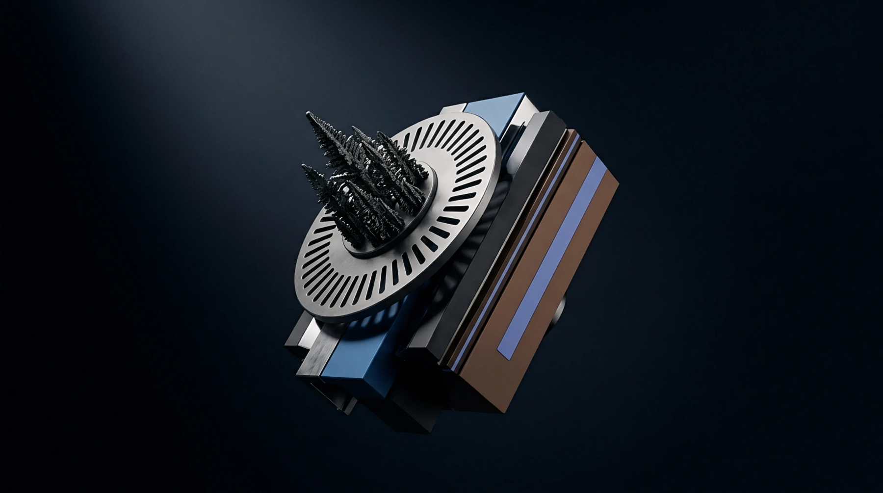
Microscopic contact regions determine the true electrical interface area between two mating metal surfaces. These spots, termed a-spots, are the only physical locations where current can cross the boundary between conductive terminals. They shrink or expand in response to mechanical pressure and surface finish, establishing the limits of electrical conductivity.
Interface Physics
Surface asperities deform plastically or elastically when two connector pins are pressed together. Under high force, the micro-protrusions flatten to increase the diameter of individual conductive zones, which helps distribute the electric current more evenly. These microscopic contact areas, known as a-spots, penetrate surface oxides to establish clean electrical pathways.
Because their total area is extremely small, current lines are forced to bunch together as they flow through these narrow bottlenecks.
Constriction Resistance
Electrical resistance rises when current flows through extremely narrow conductive channels. This phenomenon, heavily influenced by the distribution of a-spots, results in localized heating that can compromise the mechanical integrity of the terminal. If the temperature exceeds a critical threshold, the metal softens or melts, which alters the physical contact area and can cause terminal welding.
Circuit designers calculate this resistance by measuring terminal voltage drop under a calibrated test current.
Mechanical Load
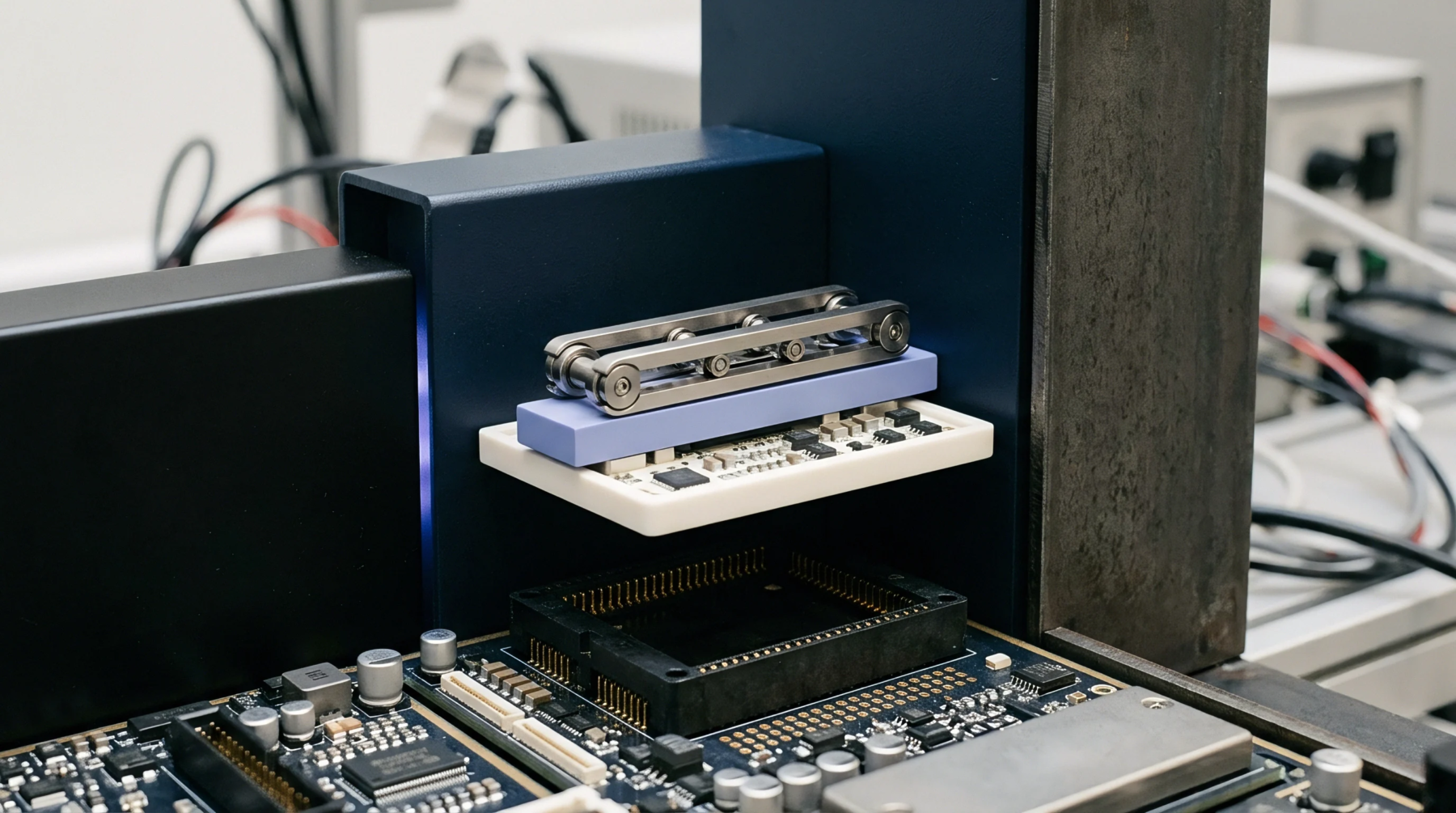
Physical force applied to a connector assembly determines the stability of the conductive paths. With inadequate force, the a-spots are unstable and highly sensitive to external vibrations. This instability causes fluctuations in signal transmission and can lead to intermittent open circuits in high speed digital assemblies.
Over time, environmental oxidation diminishes the active conducting area unless sufficient normal force is maintained to fracture new surface layers.