Designing Automated Contact Interface Boards for High Volume Semiconductor Testing
Designing automated contact interface boards for high-volume semiconductor testing requires balancing pin wiping mechanics, high-frequency signal integrity, and mechanical stiffener design to prevent substrate deflection under multi-hundred-kilogram contactor loads.

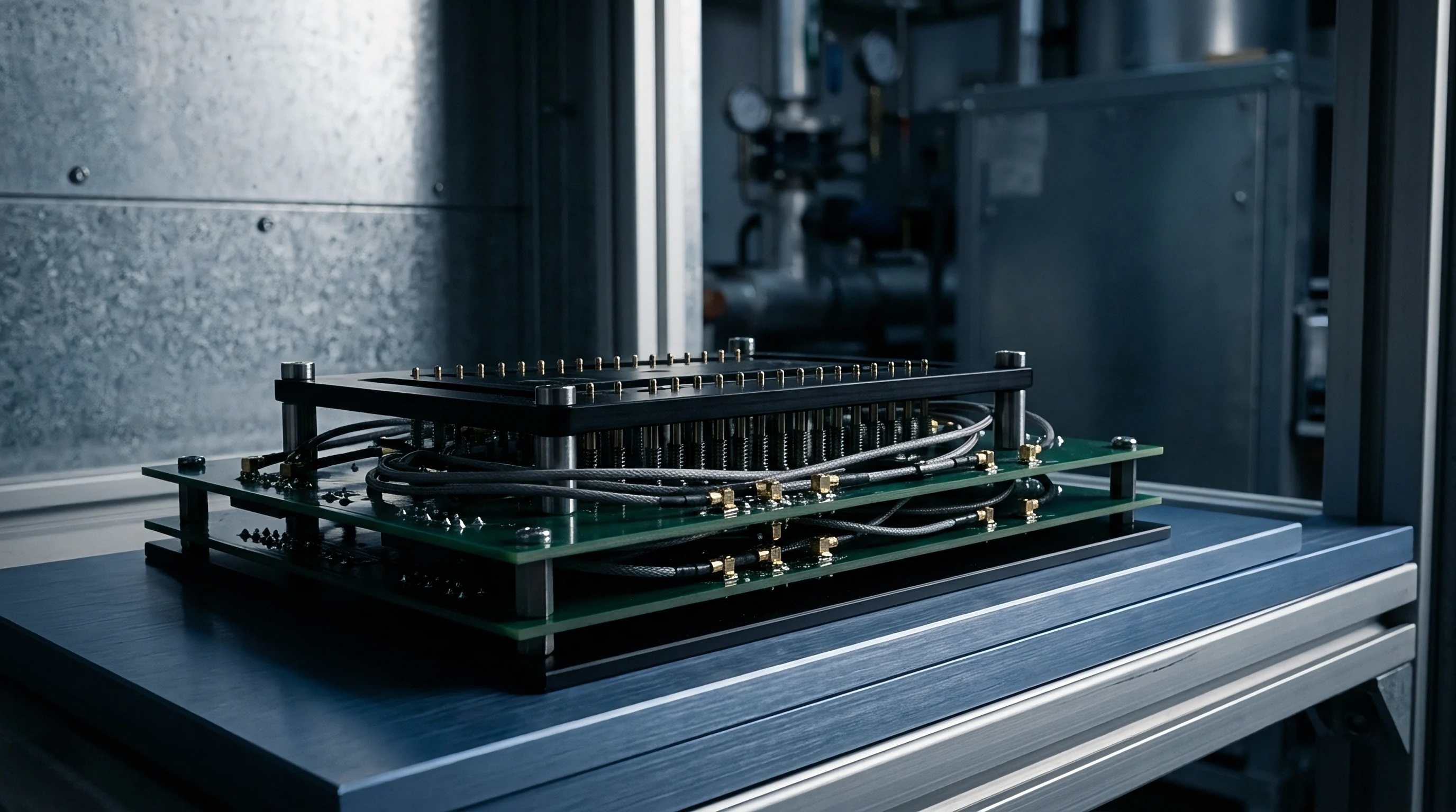
Socket
Automated test equipment relies on mechanically compliant pins to bridge the physical gap between silicon die test pads and printed circuit assemblies. High-volume semiconductor manufacturing subjects these contact interface boards to millions of actuation cycles under rigid planar tolerances. Pin pitch reductions down to zero point three millimeters force interface board designers to re-evaluate structural deflections, contact spring pressures, and pad plating durability.
Selecting the correct contactor architecture directly governs product test yields, handler uptime, and maintenance intervals across continuous factory operations.
Pogo pins force clean metal contact. Cantilever beams and elastomer interconnects provide alternate compliance pathways, yet spring-loaded probe pins dominate automated test interfaces due to predictable force-displacement behavior. Standard contactors maintain nominal contact force between fifteen and thirty grams per pin at working travel.
In a ten-thousand-pin high-density device interface board, aggregate actuation force reaches three hundred kilograms. Uncontrolled board deflection under this massive mechanical load bows the printed circuit substrate, lifting outer pin rows out of coplanar alignment and causing open-circuit falsing during automated test runs.
Spring Compliance and Contact Resistance
Pogo pin actuation generates localized wiping actions that clear non-conductive surface films from target pads during gantry engagement. Electrical contact resistance remains stable when plunger tips exert sufficient normal force to penetrate microscopic surface tarnish without gouging underlying copper traces. The initial interface contact resistance averages twenty milliohms for gold-plated crown tips on immersion-gold package pads.
Pogo pins force clean metal contact. Plunger tip geometry dictates contact pressure distribution, where four-point crown styles cut through oxidation while flat tips minimize pad cratering on delicate wafer-level chip-scale packages.
Contact wipe distance scales with pitch compression to break surface oxides without scrubbing base copper off the contact pad.
Over-compression accelerates mechanical wear and introduces permanent set in internal helical springs. Test cell gantries must maintain precise vertical z-stage position control within ten micrometers to prevent spring solid-height binding. When internal springs compress beyond recommended working stroke limits, fatigue fractures occur rapidly, increasing pin electrical resistance and introducing intermittent open faults during high-throughput test execution.

Wiping Geometry and Oxide Penetration
Plunger tip profiles determine how force concentrates across microscopic surface roughness. Spear point tips concentrate thirty grams of contact force onto a narrow tip radius, producing extreme local pressure that pierces thin aluminum oxide films on un-bumped pads. Crown tips distribute the load across multiple sharp perimeter points, providing redundant current paths that stabilize power delivery to high-current supply pins.
Self-cleaning wiping actions occur as the internal spring compresses, translating vertical stroke into a tiny horizontal sliding action across the bond pad surface.
Oxide layers impede electron flow. Debris accumulation inside plunger tip cavities degrades wiper mechanics over time. Lead-free solder ball alloys, such as tin-silver-copper, transfer soft solder material onto probe tips during thermal test cycles.
Soft solder transfers coat hard gold plating, increasing contact resistance from milliohm baselines up to several ohms within fifty thousand contact actuations. Automated interface board maintenance schedules require periodic offline ultrasonic solvent cleaning and mechanical brush cycles to strip accumulated solder residues from contactor tips.
- Plunger Tip Wear transfers soft solder alloy onto probe points, increasing contact resistance and triggering false device rejections during high-volume production testing.
- Spring Fatigue Fracture reduces localized normal force below the threshold required to pierce surface oxide layers, causing intermittent power droop during heavy device current steps.
- Substrate Board Bowing distorts overall interface coplanarity, preventing outer pin perimeters from reaching specified working travel under full gantry compression.
- Housing Cavity Contamination locks internal spring plungers in compressed positions, creating permanent open circuit conditions across affected automated test paths.
Failing to account for cumulative contact compression force causes substrate flexure that lifts perimeter pins, destroying test repeatability across high-density device sockets.
Signal
High-speed automated testing demands exact trace geometries to preserve edge rates down to the picosecond regime. Signal degradation destroys yield. Modern system-on-chip test interfaces pass digital data rates exceeding thirty-two gigabits per second alongside microwave radio frequencies above forty gigahertz.
The contact interface board functions as a high-performance transmission lines unit, where every via, pin launch, trace transition, and decoupling capacitor layout governs overall signal integrity.
Impedance discontinuities along the test channel induce signal reflections that corrupt eye diagrams and distort bit error rate measurements. Dielectric materials selected for high-speed automated interface boards require low dissipation factors and stable dielectric constants across broad operating temperature ranges. Fiber weave effects in conventional FR-4 laminates cause differential skew when parallel trace pairs align unevenly over glass yarn bundles.
Specifying spread-glass reinforcement fabrics with low-loss resin systems mitigates phase velocity imbalances across long interface board routes.
Impedance Matching across Dielectric Substrates
Controlled dielectric constant laminates limit velocity variations across parallel transmission paths. Single-ended interface traces are designed for fifty-ohm characteristic impedance, while differential pairs target eighty-five or one-hundred-ohm differential impedance based on test instrument receiver requirements. Trace width tolerances must remain within five percent of target dimensions across the entire board surface to avoid localized impedance dips that degrade high-frequency return loss performance.
Differential insertion loss across thirty gigahertz test paths increases by two tenths of a decibel per millimeter when fiberglass weave pitch aligns with trace routing vectors.
Ground planes damp crosstalk noise. Interstitial ground vias placed adjacent to high-speed signal vias form shielded vertical coaxial transitions through multilayer circuit boards. Without surrounding ground shielding vias, vertical signal transitions through thick interface substrates create unwanted electromagnetic coupling into adjacent test channels, raising background noise floors and narrowing jitter margins on sensitive device outputs.
Can Blind Vias Eliminate Stub Reflections at Forty Gigahertz?
Back-drilling removes unused copper lengths from multilayer printed circuit boards to prevent high-frequency resonance spikes. Unused via stubs behave as open-ended transmission line branches that resonate at specific frequencies, creating deep insertion loss notches in the channel spectrum. Controlled-depth back-drilling leaves stub lengths below one hundred micrometers, shifting stub resonances far beyond the active bandwidth of thirty-two gigabit per second test signals.
Blind and buried via architecture eliminates unused via stubs entirely by restricting vertical transitions to active signal layer spans. Sequential laminate buildup processing enables microvia stackups directly beneath surface contactor pads, offering direct vertical routing without long z-axis drill barrels. High-density interconnect technology allows interface boards to route thousands of high-speed test channels out from ultra-fine-pitch contactor footprints without introducing uncontrolled trace stubs or excessive layer transitions.
| Material Grade | Dielectric Constant (10 GHz) | Dissipation Factor (10 GHz) | Glass Transition Temp (°C) | Moisture Absorption (%) |
|---|---|---|---|---|
| High-Tg FR-4 | 4.25 | 0.0160 | 175 | 0.15 |
| Enhanced Epoxy (Megtron 6) | 3.71 | 0.0020 | 185 | 0.05 |
| Ultra Low-Loss Resin (Megtron 7) | 3.35 | 0.0012 | 210 | 0.03 |
| PTFE Woven Glass (Taconic) | 2.97 | 0.0009 | 280 | 0.02 |
The extent to which embedded thin-film resistor termination arrays can suppress parasitic reflections at forty-five gigahertz without introducing excessive thermal noise remains under active evaluation across interface development labs.

Thermal
Power dissipation during high-volume burn-in testing creates substantial temperature gradients across the printed assembly. Thermal stress bends thin boards. High-power graphics processors, artificial intelligence accelerators, and automotive power modules draw hundreds of amperes during active automated test routines, elevating local contactor temperatures beyond one hundred fifty degrees Celsius.
Uncontrolled heat expansion causes dimensional shifts that misalign pogo pin arrays relative to silicon die contact pads, risking severe mechanical damage to test hardware.
Copper expands under heavy load. The coefficient of thermal expansion mismatch between organic printed circuit boards, metallic contactor housings, and silicon device substrates generates lateral shear stress across probe pin tips. Standard FR-4 laminates expand laterally at fourteen to seventeen parts per million per degree Celsius, whereas silicon expands at roughly two point six parts per million.
When test temperatures swing from sub-zero automotive qualification levels of minus forty degrees up to hot testing at one hundred twenty-five degrees, differential thermal expansion slides probe tips off narrow bond pads.
Active Load Dissipation and Structural Expansion
High current draw induces localized heat spikes that warp organic substrate materials. Heavy copper power layers within interface boards conduct heat laterally away from central contactor zones toward perimeter mounting frames. Interface board designs incorporate solid copper thermal planes, copper-filled thermal vias, and embedded aluminum or copper heat-sink plates directly behind high-current device sockets to dump heat into handler thermal conditioning units.
Standard IPC 6012 Class 3 insulation resistance limits mandate clean dielectric surfaces under five hundred volts direct current bias before thermal cycling begins.
Clean power pads reduce droop. Thermal relief traces on high-current power vias are avoided in automated test boards because thermal ties add parasitic inductance and electrical resistance. Continuous power planes are connected directly to via barrels using full thirty-six0-degree plane connections, requiring heavy-duty soldering equipment during manufacturing board assembly to achieve proper solder reflow around massive thermal copper masses.
Coefficient Matching across Composite Stackups
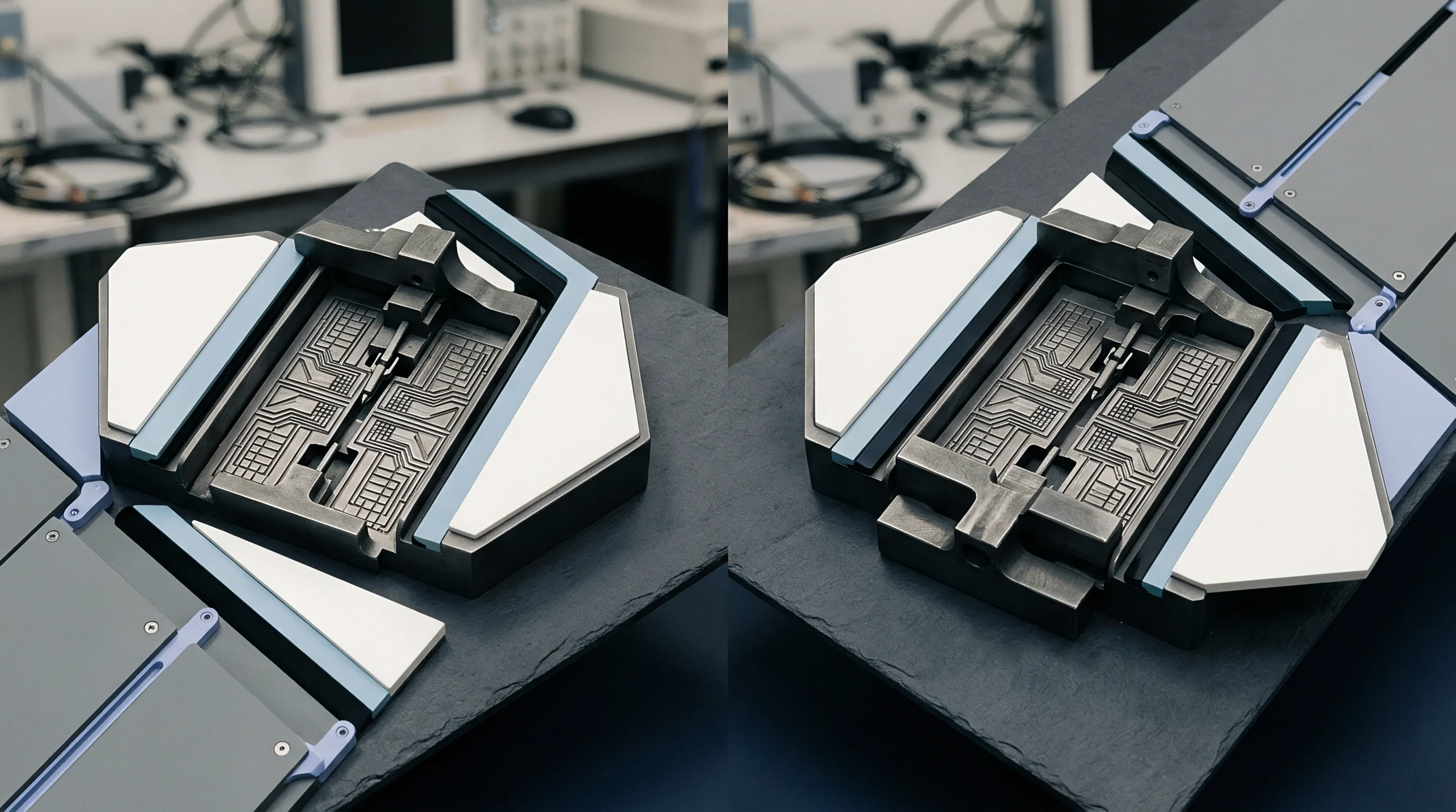
Mismatched expansion rates between glass-reinforced epoxies and stiffening backplanes generate inter-layer shear forces. Stainless steel or copper-invar-copper core stiffeners are bolted to interface boards to lock planar dimensions during extreme temperature swings. Low-expansion metallic stiffeners hold z-axis substrate bow within fifty micrometers across operational temperature ranges, preserving coplanarity between contactor housings and test head docking interfaces.
- Thermal Expansion Coeffcient Matching requires selecting composite stiffener materials whose lateral expansion aligns with silicon die characteristics to prevent probe tip walk during temperature transitions.
- Direct Power Plane Coupling eliminates thermal relief cutouts around high-current vias to lower electrical impedance and improve localized heat conduction into internal copper layers.
- Active Cooling Duct Alignment routes handler liquid or forced-air cooling paths directly through stiffener cutouts to prevent hot-spot formation behind high-power test sockets.
- Z-Axis Bow Stiffening Assemblies constrain board flexure under heavy thermal loads using precision-machined aluminum or stainless steel backplanes secured with isolated mounting hardware.
Fabrication suppliers frequently attribute early layer delamination inside high-power interface boards to customer thermal test profile ramp rates exceeding specified substrate expansion thresholds.

Drift
Continuous mechanical cycles degrade mechanical alignment and electrical continuity over extended production runs. Wear changes contact force values. Contact interface boards undergo hundreds of thousands of docking actions, causing subtle mechanical shifts, pin height wear, plating transfer, and particulate contamination.
Without precise routine measurement and calibration strategies, subtle contact degradation manifests as unexplained test yield loss, driving up false failure rates and consuming valid semiconductor inventory.
Automated contactor health monitoring tracks contact resistance changes across every individual pin channel during live production testing. Test systems record continuity resistance trends, flagging specific channels that exceed defined resistance limits before catastrophic electrical opens occur. Periodic planarization measurement validates that test head gantries apply uniform downward force across all contactor quadrant positions, avoiding unbalanced mechanical loads that accelerate localized pin degradation.
Planarization Measurement and Alignment Calibration
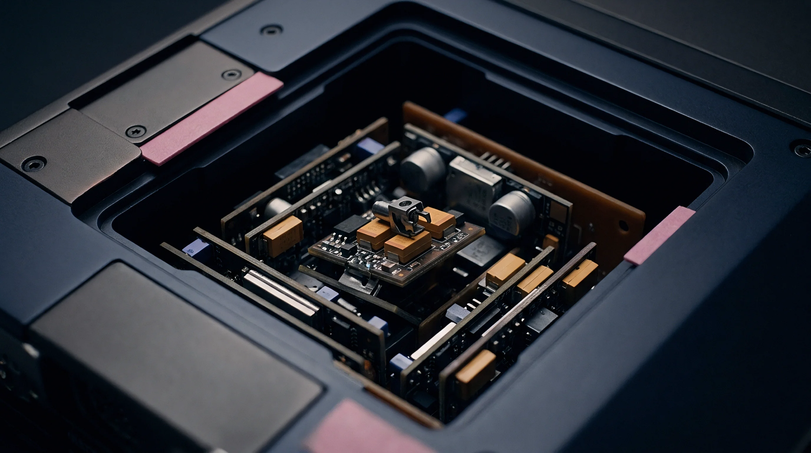
Laser displacement sensors measure surface tilt across high-density pin arrays before locking test heads into position. Physical alignment frames utilize hardened steel dowel pins and precision bushings to repeatably orient contactor housings relative to handler device positioners within five micrometers lateral tolerance. Mechanical alignment features must withstand repeated high-speed docking impacts without developing physical slop or gouging locator holes.
Gold plating resists initial oxidation. Mechanical scrubbing eventually wears away thin gold flash layers, exposing nickel underplating and beryllium-copper base alloys to atmospheric oxygen. Exposed base metals form resistive oxide films rapidly, causing contact resistance to drift upward from tens of milliohms to multiple ohms.
Optical inspection tools identify plating wear patterns on plunger tips, enabling predictive pin replacement before contact drift impacts factory yields.
Plating Degradation and Cleaning Routines
Scrubbing action transfers pad debris onto plunger tips, raising electrical impedance over successive actuations. Offline maintenance procedures utilize automated pin cleaning stations equipped with micro-abrasive elastomer sheets or shaped brass brushes. Contactors compress into cleaning media for specified cycle counts, clearing accumulated solder flakes and organic flux residues from plunger tip contours without stripping underlying hard gold plating layers.
- Mount the interface board onto an offline optical alignment bench and lock the stiffener backplane to the primary datum structure.
- Engage a multi-axis laser displacement transducer across the four corners of the socket housing to capture baseline planarity coordinates under zero load.
- Apply a calibrated three-hundred-kilogram mechanical test load to the central contactor housing while recording board deflection across perimeter displacement sensors.
- Adjust vertical micrometer shims behind the stiffener mounting pads until total surface tilt remains below twenty-five micrometers across the entire pin matrix.
Under IPC-A-610 Class 3 acceptance criteria, any interface board displaying contact pad copper exposure exceeding fifteen percent of the active contact area requires immediate removal from production service for re-plating or board replacement.
Sourcing
Procurement contracts for high-volume automated test interface hardware split responsibilities between design owner and fabrication house. Test speeds demand low loss. Solder joints fracture under flex.
Translating high-density silicon test requirements into fully qualified interface board hardware involves non-recurring engineering fees, complex stackup fabrication proofs, custom contactor housing tooling, and strict signal integrity acceptance testing. Sourcing managers must define explicit boundaries between turnkey scope handoffs and semi-custom engineering splits to prevent unexpected cost overruns and operational delays during production bring-up.
Turnkey interface board programs hand complete execution responsibility to a specialized interface design house. The buyer provides device pinouts, package mechanical drawings, handler docking specs, and ATE channel maps. The engineering house executes schematic design, stackup simulation, high-speed trace routing, stiffener mechanical modeling, fabrication file generation, board assembly, and final laboratory signal verification.
Semi-custom scope models split these deliverables, leaving schematic generation and signal integrity simulation with the buyer while offloading physical board layout, fabrication, and mechanical assembly to external manufacturing partners.

Non-Recurring Engineering Breakdown and Deliverables
Upfront design fees cover schematic generation, stackup modeling, signal integrity simulations, and drill tool generation. Non-recurring engineering costs for high-density, thirty-two-layer interface boards equipped with back-drilled blind/buried vias range from thirty thousand to over one hundred thousand dollars depending on channel counts and operating frequency bands. Tooling expenses include custom drill bits, electrical test fixture construction, mechanical stiffener CNC machining, and contactor alignment housing molding.
Uncompressed pogo pin heights vary by fifteen micrometers across a single hundred-pin matrix after fabrication tolerances accumulate.
Design ownership governs future manufacturing flexibility. When buyers contract interface development under turnkey terms without securing native CAD design files, Gerber fabrication outputs, drill tables, and stiffener mechanical step files, they bind future board builds to a single supplier. Sourcing contracts must mandate full delivery of open-format IPC-2581 or ODB++ design transfer packages alongside native schematic databases, enabling secondary fabrication facilities to build replacement interface boards without repeating costly non-recurring engineering cycles.
Turnkey and Semi-Custom Scope Boundaries
Interface board procurement requires clear file handoffs to ensure second-source manufacturing options remain viable. Scope boundary ambiguities frequently arise during high-speed signal integrity validation. If a turnkey supplier guarantees eye-diagram performance at forty gigahertz, acceptance testing must occur on calibrated laboratory vector network analyzers using standardized launcher fixtures before board shipments receive formal sign-off.
| Engineering Deliverable Item | Turnkey Scope Owner | Semi-Custom Scope Owner | Mandated File Format | Acceptance Criterion |
|---|---|---|---|---|
| Schematics & Netlists | Supplier | Buyer | Native CAD / EDIF | Zero short/open netlist mismatches |
| SI / PI Simulation Dossier | Supplier | Buyer | Ansys Touchstone / IBIS | Insertion loss < 2dB at 30GHz |
| PCB Fabrication Outputs | Supplier | Supplier | IPC-2581 / Gerber X2 | IPC 6012 Class 3 inspection pass |
| Stiffener Mechanical CAD | Supplier | Supplier | STEP / Parasolid | Planarity < 25µm under full load |
| Contactor Assembly Drawings | Supplier | Supplier | PDF / Native CAD | 100% pin position optical check |
| Methods note: Deliverable transfer sign-off mandates physical verification using calibrated time-domain reflectometry and optical CMM inspection prior to invoice settlement. | ||||
Price breakdowns for high-volume interface boards separate raw fabrication costs, contactor housing assembly, mechanical stiffeners, and individual pogo pins. Pogo pins represent a major recurring cost driver in ultra-high-density contactors, where high-performance crown pins cost between one and three dollars per channel. In an eight-thousand-channel interface board, contactor pin volume alone contributes over sixteen thousand dollars to total unit hardware bill of materials, making pin cycle life warranties and pin replacement kit availability vital clauses in commercial supply agreements.