Initial Contact Resistance Baseline Verification in Test Sockets
Initial contact resistance verification isolates test socket wear to prevent false radio parametric failures and secure accurate module production yields.


Pin
Contact resistance across automated test interface hardware governs measurement accuracy on radio frequency module lines. When screening wireless parts running WiFi 6, Bluetooth Low Energy, or cellular chipsets, the physical interface between the device under test and the test fixture introduces parasitic resistance. Known in test engineering simply as contact resistance, this metric combines the bulk resistance of the spring contactor material, constriction resistance across microscopic asperities at the mating surface, and film resistance from oxides or debris.
Establishing an accurate baseline for pristine contactors before production cycling begins is the only reliable way to separate silicon flaws from deteriorating socket tooling.

Primary Conduction Interfaces in Production Contactor Arrays
Automated test equipment interfaces with miniature solder balls or perimeter land grid arrays through micro-machined spring elements, typically pogo pins or cantilever beam contacts, that establish galvanic connection with package terminals. Machined polymer blocks made from Torlon or PEEK house dozens of these pins in tight arrays. Inside each pin barrel, an internal spring supplies the normal force required to punch through surface oxides that would otherwise impede electron transport.
A gold-plated beryllium copper spring contactor exhibits an initial resistance baseline between 18 and 35 milliohms under 30 grams of vertical pre-load before mechanical cycling commences.
Actual mechanical engagement occurs across microscopic high spots termed a-spots rather than the apparent surface area of the terminal, meaning constriction resistance dominates the junction. Applying higher mechanical force flattens and enlarges these discrete conduction points, driving constriction resistance down in line with Holm contact theory. Plating stacks ~ usually hard gold over a nickel diffusion barrier ~ shield the underlying beryllium copper or tellurium copper core from atmospheric tarnishing, though micro-scale surface roughness still creates measurable resistance differences between adjacent pins in the array.
Several early-life mechanical failure modes degrade these physical junctions directly:
- Plating micro-fissuring occurs when localized mechanical shear fractures brittle hard-gold layers during initial socket actuation cycles.
- Spring relaxation reduces contact normal force below design thresholds after brief thermal exposure during automated device testing.
- Housing cavity misalignment tilts the central plunger axis, causing uneven mechanical force distribution across opposite package corners.
- Contaminant transfer deposits volatile organic outgassing from circuit board substrates onto clean contactor crowns during initial insertions.
When contactors wear and baseline verification is neglected, variations in contact force propagate through the fixture unnoticed, generating false parametric failures that scrap perfectly good radio hardware.
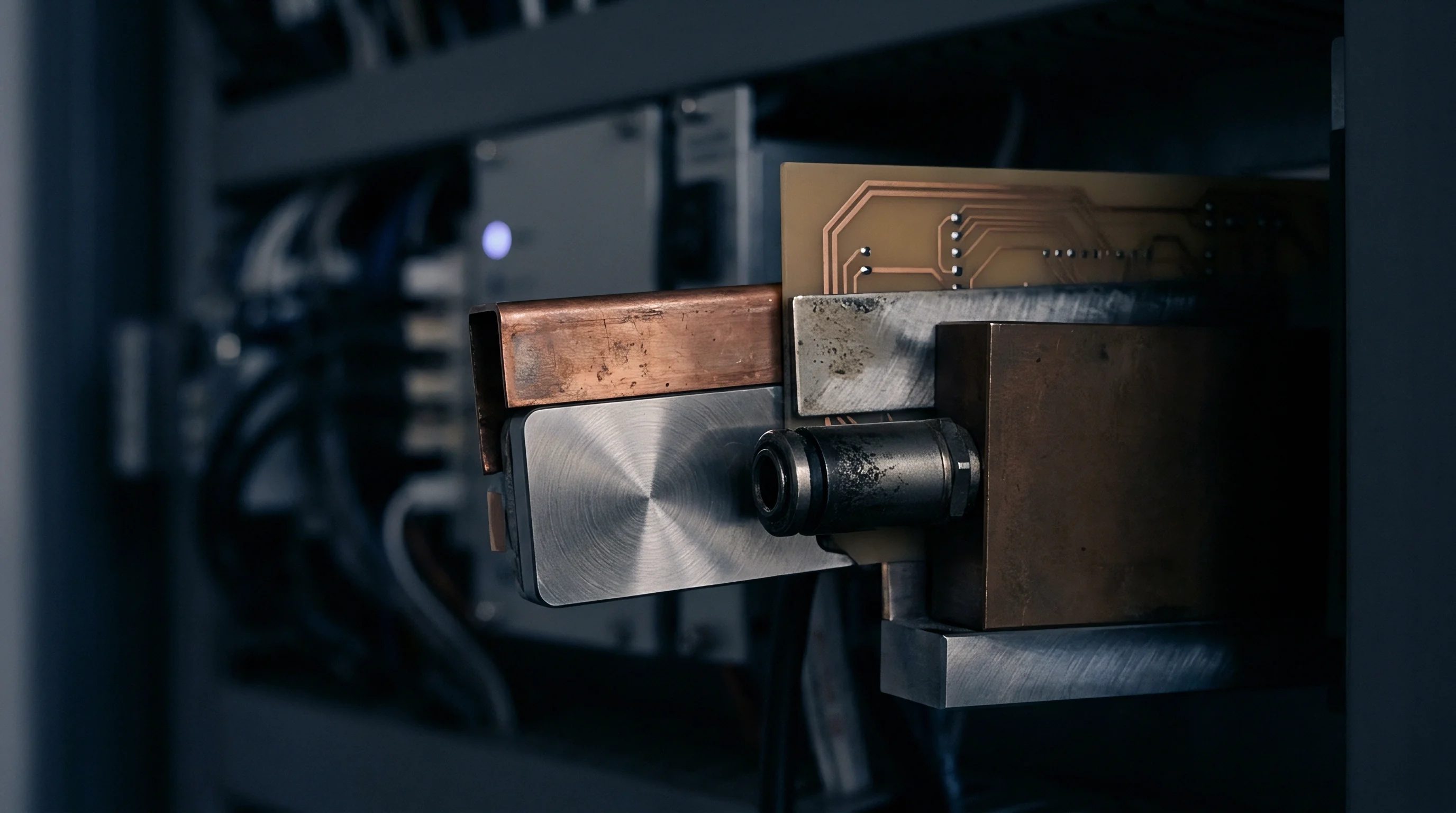

Scrub
Mechanical displacement between spring contactor tips and package lands cuts through passive surface oxides during vertical travel. As the test handler pushes the module down into the socket, the contact geometry drives a brief horizontal wipe across the pad metallization ~ an action known as scrub. This horizontal shear displaces surface contaminants and exposes fresh metal to lower interface resistance, though excessive wiping risks wearing the protective gold down to the nickel barrier and undermining signal integrity.

What Drives Initial Contact Resistance Variation across RF Pins?
Variations in plating thickness and small tooling tolerances alter the microscopic constriction zone the moment the probe touches solder. Crown tip shapes, like four-point crowns or chisel profiles, concentrate normal force onto tiny contact points. The mating surface matters just as much: flat lands on land grid array modules present different roughness profiles depending on whether the board uses electroless nickel immersion gold or organic solderability preservatives.
Immersion gold yields quickly with minimal scrub distance, whereas solder balls on ball grid arrays deform plastically, requiring a specific wipe vector to keep displaced solder from loading up the pin crown.
Radio frequency return paths through ground pins alter measured amplifier power long before direct current continuity registers an open circuit.
Radio frequency test pins are especially unforgiving of contact resistance drift. A 50-milliohm shift on a DC supply rail merely nudges the bias voltage, but that same resistance on an RF ground return alters return inductance and degrades transmission line impedance. The resulting mismatch drives up reflection losses, inflates error vector magnitude on wideband WiFi 6E channels, and cuts into measured sensitivity on sub-GHz LoRa links.
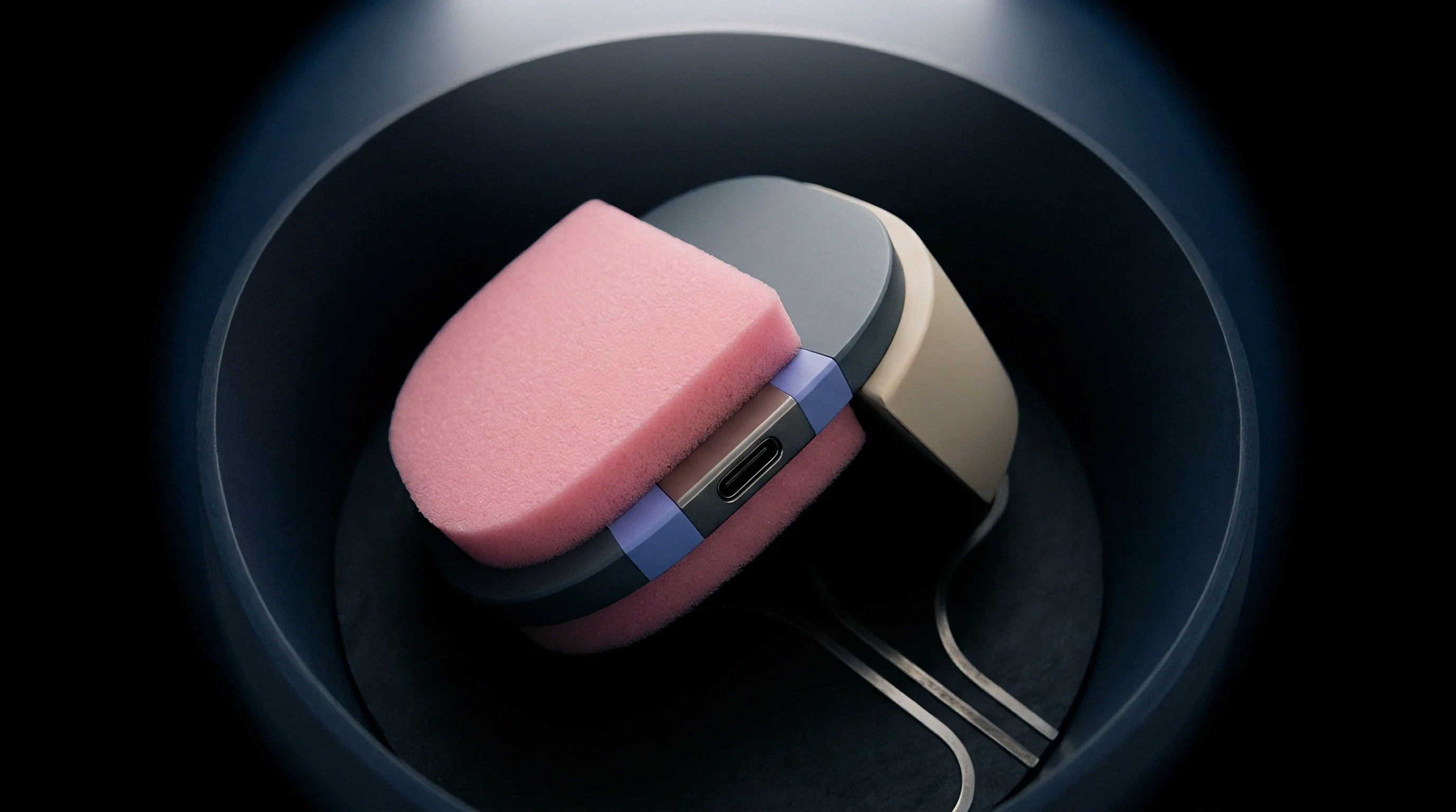
Mechanics of Contactor Tip Displacement on Solder Lands
Cantilever and angled probe designs deliberately sweep between five and twenty micrometers across the metallized pad during touchdown to clear debris left by previous cycles. Vertical pogo pins with internal biasing lines create a slight twisting motion during compression instead, getting the scrub needed to prevent receiver corruption from ground bounce without pushing outward on the socket body.
| Contactor Architecture | Contact Normal Force | Initial Baseline Resistance | Loop Inductance | RF Bandwidth at -1 dB | Mechanical Cycle Rating |
|---|---|---|---|---|---|
| Cantilever Kelvin Beam | 25 to 35 gf | 15 to 25 mΩ | 0.8 to 1.2 nH | 6.5 GHz | 150,000 cycles |
| Biased Pogo Spring Pin | 30 to 45 gf | 20 to 35 mΩ | 1.1 to 1.6 nH | 10.0 GHz | 250,000 cycles |
| Conductive Elastomer Column | 15 to 25 gf | 35 to 60 mΩ | 0.2 to 0.4 nH | 40.0 GHz | 50,000 cycles |
| Coaxial Spring Contactor | 40 to 60 gf | 12 to 20 mΩ | 0.5 to 0.8 nH | 18.0 GHz | 200,000 cycles |
Choosing a tip geometry always involves a compromise between scrub aggressiveness and pad wear. Sharp chisel points slice cleanly through tough oxides on lead-free solder alloys, but they also shed their gold plating much faster, accelerating base-metal diffusion underneath.

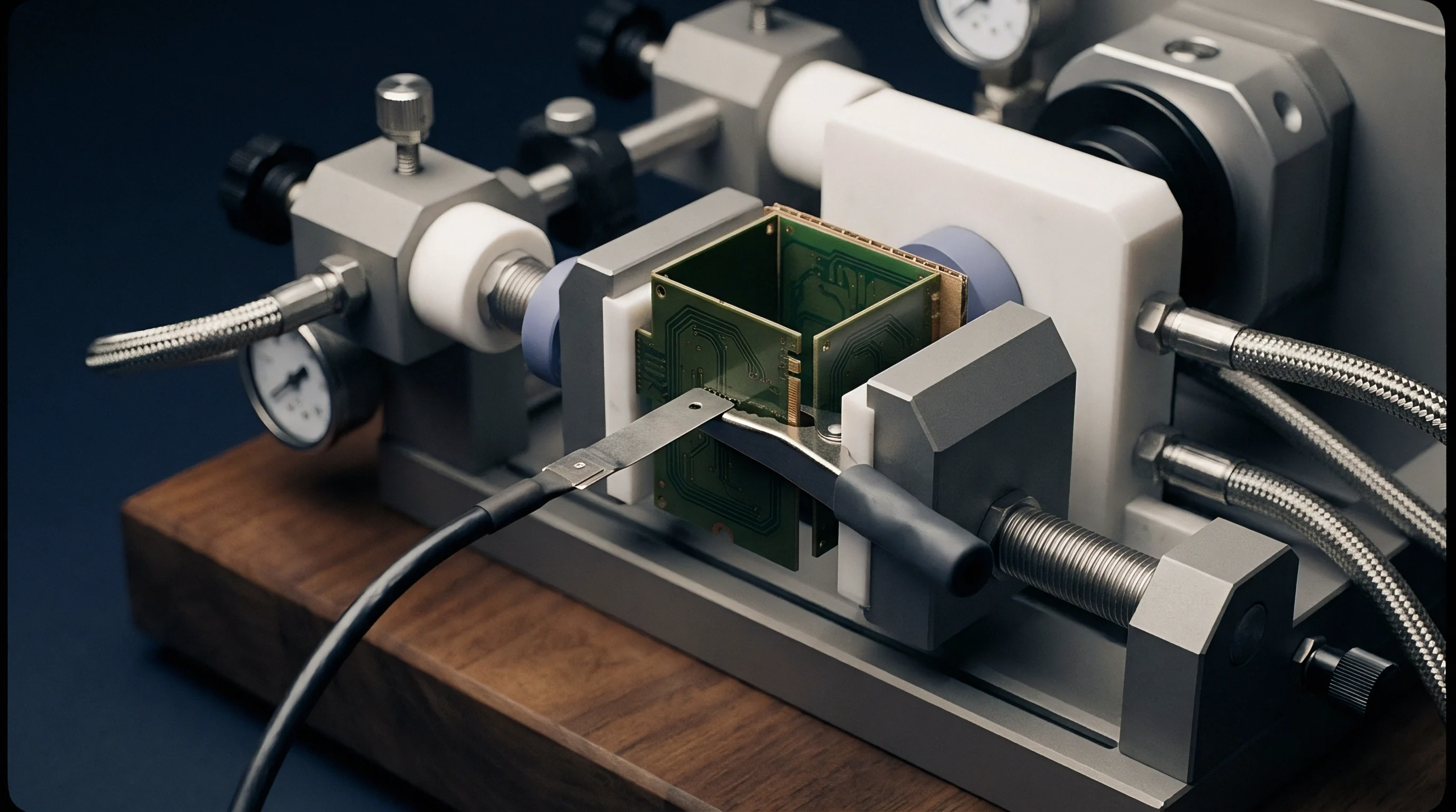
Coupon
Precision gold-plated shorting plates provide the baseline reference required to calibrate test fixtures before running production lots. Instead of inserting a live module, operators seat a dedicated verification artifact ~ often called a shorting block or gold coupon ~ that matches the mechanical envelope of the radio package. These coupons are machined from copper or aluminum alloys, plated with heavy electrolytic nickel, and finished with at least 1.25 micrometers of hard gold to withstand repeated contact engagement.

Four-Wire Kelvin Implementation on Planar Standard Blocks
Routing sense traces directly to the socket separates trace parasitics on the board from the contact interface itself. Two isolated paths run to the pin under test: one delivers the excitation current while the other reads voltage drop. Because the high-impedance voltmeter pulls virtually no current through the sense line, the reading isolates the contactor assembly and coupon interface without lead resistance skewing the data.
Adherence to ASTM B539 test methods for dry-circuit resistance prevents electrical breakdown of contact films and protects baseline data integrity.
Dry-circuit standards dictate initial contact resistance testing parameters. Instrument limits cap open-circuit voltage at 20 millivolts and current at 100 milliamperes or less, ensuring thin insulating films do not rupture via fritting. If excessive voltage punches through an oxide layer via dielectric breakdown, the meter records a deceptively low resistance value that conceals physical contact wear.
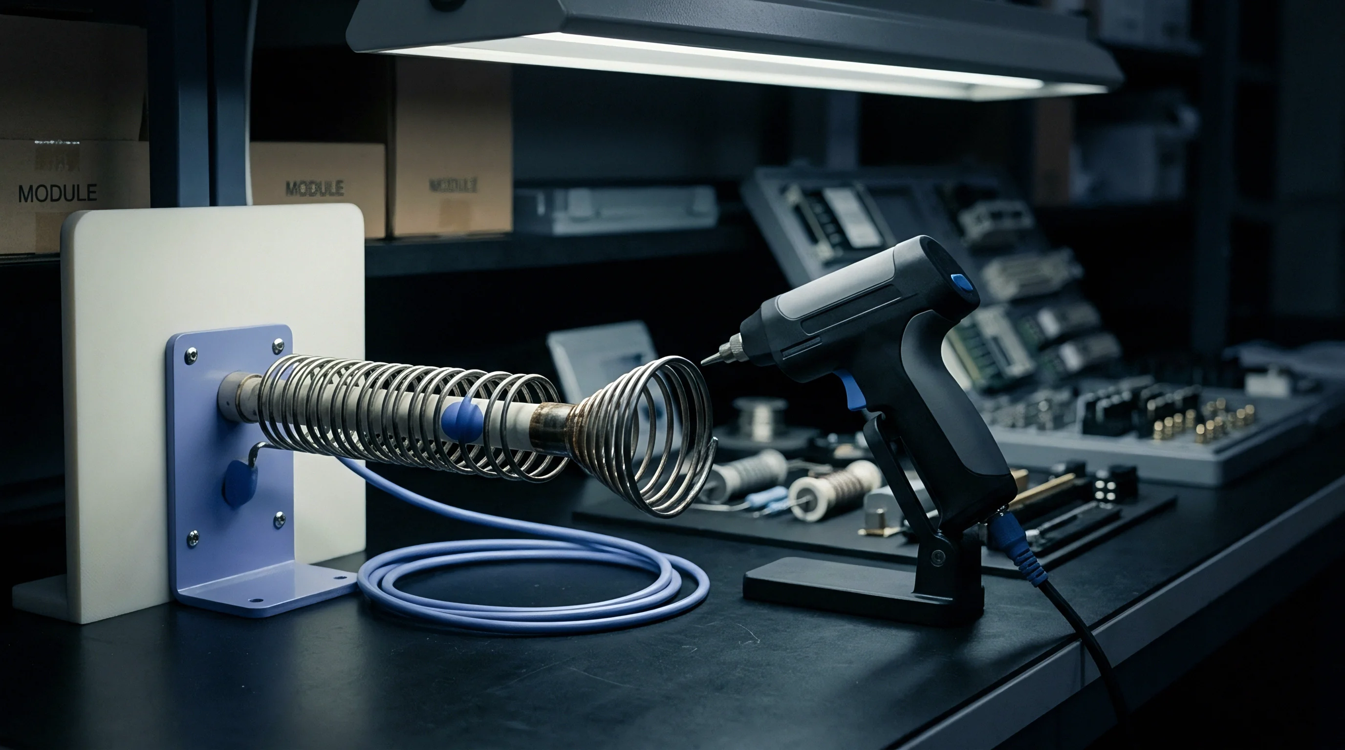
Diagnostic Sequencing for Baseline Fixture Acceptance
Before any production modules are tested, the system runs automated continuity sweeps through every signal path using a standardized fixture qualification routine:
- Dry-circuit four-wire baseline capture records initial unpowered contact resistance across every socket pin using current-limited instrumentation.
- Actuation force profiling measures the vertical load displacement curve to confirm that socket springs deliver nominal contact pressure at working travel.
- Gold shorting block planarization check confirms uniform mechanical touchdown across all four package quadrants using pressure-sensitive film.
- Multi-insertion statistical spread calculation executes fifty consecutive coupon actuations to establish baseline mean values and standard deviations for every pin.
Standard blocks require regular inspection for gold pickup and mechanical scoring, and tight machining tolerances prevent the pins from binding during alignment. MIL-STD-202 Method 307 sets a strict fifty-milliamp test current ceiling to avoid arcing across these calibration surfaces.


Offset
Systematic parasitic resistance across a test socket distorts both DC power delivery and high-frequency RF returns. Test programs typically build in software offsets to cancel out predictable fixture resistance; for instance, if a clean socket pin on a supply rail measures 22 milliohms during qualification, the test executive subtracts that value from raw voltage drop readings. Unchecked insertion loss on high-frequency lines will still degrade receiver noise figures.

Why Do Baseline Kelvin Offsets Degrade during Thermal Cycles?
Mismatch in thermal expansion between polyimide socket housings and copper-alloy pins shifts the seating angle at temperature extremes. Industrial wireless devices regularly undergo qualification testing from -40 degrees Celsius to +85 degrees Celsius. As the fixture heats up, friction inside the pin barrels climbs, reducing spring stroke and contact force so that baseline resistance calibrated at 25 degrees Celsius drifts upward.
Solder migrating from module pads to the probe tips compounds this drift across hundreds of temperature ramps.
Thermal stress accelerates tin migration from lead-free solder residue into the probe’s gold layer, creating intermittent yield fallout. This diffusion forms brittle, resistive gold-tin intermetallics such as AuSn and AuSn4, whose bulk resistivity can run ten times higher than virgin gold and cause sudden, steep jumps in contact resistance.
| Wireless Protocol Standard | Monitored Test Parameter | Nominal Specification Limit | CRES Drift Threshold | Induced Measurement Defect |
|---|---|---|---|---|
| BLE 5.4 Low Energy | Deep Sleep Current Consumption | 1.2 μA maximum | +150 mΩ on VDD | False current spikes from bias noise |
| WiFi 6 (802.11ax) | Transmit Error Vector Magnitude | -35 dB at MCS11 | +80 mΩ on RF Ground | False EVM floor degradation |
| LoRaWAN SX1262 | Receiver Sensitivity at SF12 | -137 dBm at 125 kHz | +120 mΩ on LNA input | 0.8 dB apparent sensitivity loss |
| LTE-M (3GPP Cat-M1) | Maximum Output Power (+23 dBm) | 23.0 dBm ± 0.5 dB | +60 mΩ on PA supply | 0.4 dB power slump during bursts |

Parametric Measurement Distortion across Wireless Standards
Stray resistance along power lines creates immediate voltage droop during peak RF bursts. An LTE Cat-M1 module can draw up to 500 milliamperes in transmit mode. If barrel wear or contamination pushes the supply pin’s resistance from a 25-milliohm baseline up to 200 milliohms, the module sees an instantaneous 100-millivolt droop at the package pad, tripping brown-out circuits or degrading power amplifier linearity enough to fail an in-spec part.
Production fixtures require documented baseline offsets before handoff to the floor:
- Loop inductance mapping records high-frequency impedance profiles across every coaxial contactor channel using a vector network analyzer.
- Kelvin bridge residual records log contactor baseline resistances alongside ambient temperature and relative humidity telemetry.
- Cleaning interval triggers define the maximum allowable resistance deviation before automated scrub brushes clean pin tips.
- Gold-tin intermetallic warning bands flag socket pins whose resistance fails to return to baseline after ultrasonic solvent cleaning.
Current probes expose these parasitic drops, though whether dry-circuit routines alone can anticipate RF insertion loss shifts across temperature without putting a network analyzer on every pin remains an active technical debate.

Yield
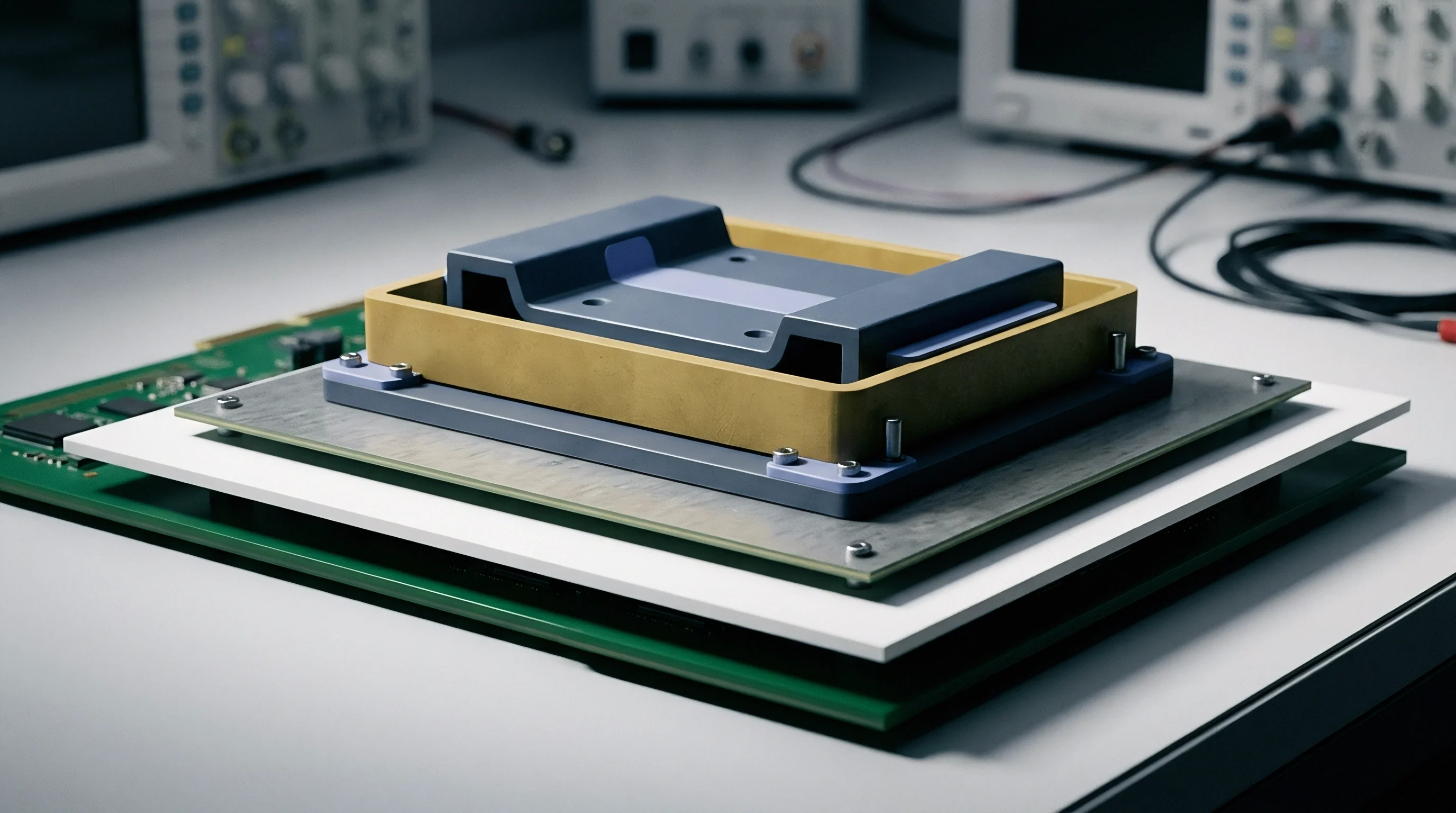
Factory economics hinge on distinguishing true silicon defects from socket wear. On high-volume assembly lines, first-pass yield is tracked constantly; when socket pins collect oxide skins, debris, or mechanical scoring, their resistance climbs and drags down parametric RF performance, generating artificial yield losses.
Worked Economic Model for False Rejection Overhead
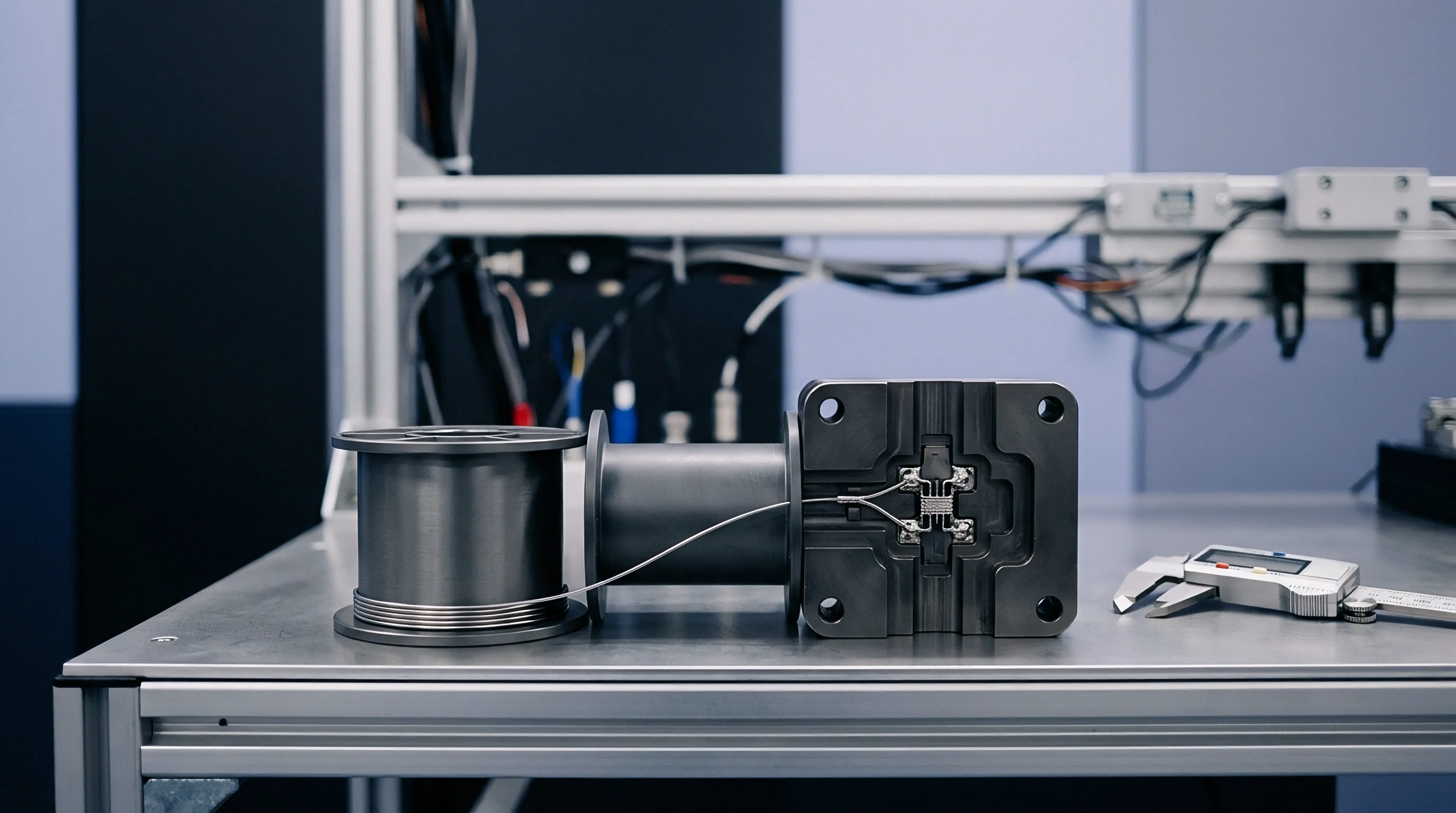
Consider a 50,000-unit lot of dual-band WiFi 6 modules running on a quad-site automated test cell. Each assembled module carries a bill-of-materials cost of $4.50. Test cycle time runs 18 seconds of handler index time per part, backed by tester operational costs of $65.00 per hour across the four sites.
Unchecked socket drift that introduces 90 milliohms of parasitic resistance to the RF ground pins on just two test sites creates measurable financial damage:
The elevated ground impedance degrades measured channel 7 transmitter EVM from an actual -36 dB down to -33 dB. Because the test program cuts off at -35 dB, the false reject rate on those two degraded sites rises by 2.4 percent.
Across the 25,000 units tested on those compromised sockets, 600 acceptable modules fail. Scrapping them outright represents an immediate loss of $2,700. Routing them to bench retest requires roughly four minutes of manual handling per unit; at an engineering labor rate of $42.00 per hour, rechecking 600 modules tacks on another $1,680.
That single unverified baseline shift produces $4,380 in avoidable fallout across the lot.
Replacement pins cost less than $12.00 each, and running an automated baseline check with a precision gold shorting coupon takes three minutes at the start of a shift. Catching contact degradation early saves thousands of dollars in scrap and bench analysis. While spring tension relaxes over thermal cycles and cold solder joints distort return currents, regular socket verification preserves assembly margins long before pin wear turns into a factory yield crisis.