Delta Qualification Test Matrices for Process Node Hardware Transitions
Delta qualification test matrices isolate process node change risks, balancing reduced life testing with targeted silicon stress vectors.


Transit
Process node hardware transitions occur when an integrated circuit or module migrates from a mature fabrication node to an advanced geometry, such as moving a system-on-chip from a 28-nanometer planar CMOS process to a 16-nanometer or 12-nanometer FinFET platform. Integrators often treat this migration as a routine die shrink aimed at reducing unit cost and dynamic power consumption without altering system architecture. However, shifts in transistor geometry, gate capacitance, oxide breakdown voltage, and interconnect resistance invalidate baseline qualification data.
Treating a shrink as a direct drop-in replacement introduces unquantified field reliability risks whenever the scope of physical change is miscalculated.
Within semi-custom or turnkey supply contracts, the division of engineering scope determines which party shoulders delta verification. Turnkey module integrators frequently handle a node shift as an internal manufacturing optimization, issuing an updated data sheet while withholding transistor-level qualification reports. Semi-custom arrangements leave the buyer to evaluate how the process migration affects module-level parameters, including electromagnetic compatibility, transient response, low-dropout regulator stability, and electrostatic discharge immunity.
When functional anomalies appear in final assembly after a process change, financial liability falls on the buyer.
Scoping a node transition accurately means identifying every hardware subsystem altered by smaller feature sizes. Digital logic generally gains from reduced gate delay and lower operating voltages, but analog and mixed-signal blocks experience degraded performance from lower intrinsic gain and increased channel length modulation. Power management circuits face altered pass-transistor current densities, while high-speed radio frequency interfaces require revised impedance matching networks to account for shifted pin capacitance and substrate parasitics.
The failure modes associated with process node migrations stem from physical interactions at the silicon and package interface that do not scale linearly with feature size:
- LDO Dropout Degradation occurs when reduced pass-transistor channel resistance leads to control loop instability under low-input headroom conditions, causing power supply rejection ratio collapse at high frequencies.
- Electromigration Hotspots develop inside power distribution networks where current density exceeds design limits due to thinner copper metallization layers in sub-20-nanometer interconnect stacks.
- Subthreshold Leakage Swell increases static current drain during deep-sleep states, elevating standby power consumption and accelerating battery depletion in unpowered storage.
- Parasitic Capacitance Shift alters signal propagation delay along long internal routing tracks, creating setup and hold time violations across peripheral interfaces operating at maximum clock speeds.
Quantifying these failure vectors early dictates whether a transition requires a full module redesign or a targeted delta qualification. The scope engineer establishes clear boundaries for each physical interface, confirming that mask revisions, package substrate modifications, and passive component changes carry verified test data before full production release. That boundary holds only when buyer and factory agree on which stress conditions require re-testing against the baseline node.
How does the integrator verify that the factory’s internal process shift leaves the high-speed radio interface timing and spurious emission profiles within original contractual parameters?

Physics
Transistor scaling changes fundamental semiconductor physics, forcing engineering teams to re-evaluate physical stress limits during process transitions. Planar CMOS structures at 28-nanometer nodes rely on gate oxide thickness to withstand operating voltages up to 1.8 volts or 3.3 volts on input-output lines. Moving to 16-nanometer FinFET or 5-nanometer gate-all-around architectures brings core supply voltages down to 0.75 volts or 0.6 volts as gate oxides shrink to near-atomic dimensions.
Gate oxides leak under higher electric fields, shifting the primary degradation mechanisms from classical hot carrier injection to time-dependent dielectric breakdown and bias temperature instability.
| Physical Parameter | 28nm Planar CMOS | 16nm FinFET | 5nm FinFET / GAA |
|---|---|---|---|
| Core Supply Voltage (Nominal) | 1.0V – 1.2V | 0.75V – 0.85V | 0.6V – 0.75V |
| Equivalent Oxide Thickness (EOT) | 1.2nm – 1.5nm | 0.8nm – 1.0nm | 0.5nm – 0.7nm |
| Static Leakage Power Density | 15 mW/cm² | 45 mW/cm² | 120 mW/cm² |
| ESD Breakdown Threshold (HBM) | 2000V | 1500V | 1000V |
| HTOL Thermal Acceleration Multiplier | 1.0x (Baseline) | 1.45x | 2.10x |
Bias temperature instability shifts threshold voltages over operational lifespans, especially under sustained thermal load. Negative bias temperature instability affects p-channel transistors, while positive bias temperature instability acts on n-channel devices with high-k metal gate stacks. In advanced process nodes, this threshold drift manifests at lower operating temperatures and across shorter timeframes than in planar designs, slowing transistor switching, tightening digital timing margins, and increasing the risk of logic corruption over extended deployments.
Moving a system-on-chip from 28-nanometer planar to 16-nanometer FinFET lowers Human Body Model electrostatic discharge endurance from 2000 volts to 1200 volts under identical pad layout constraints.
Electrostatic discharge and electrical overstress margins drop as geometries shrink. Smaller junction areas and thinner dielectrics limit the energy dissipation capacity of input-output clamp circuits. An electrostatic discharge event absorbed without issue by legacy 28-nanometer silicon can melt metallization traces or puncture gate oxides on a 7-nanometer device.
Semi-custom hardware designs must re-validate board-level transient voltage suppression components to prevent external surges from exceeding the lower breakdown thresholds of advanced node silicon.
Thermal power density climbs because active silicon volume shrinks faster than power dissipation falls. Localized hotspots on the die create thermal gradients across package substrates, accelerating solder joint fatigue and shifting clock skew networks. Concentrating dynamic dissipation into a smaller silicon footprint also degrades standard heatsink performance due to elevated junction-to-case thermal resistance.
Factoring in these physical constraints requires updating operational thermal limits and thermal acceleration factors during environmental stress testing.
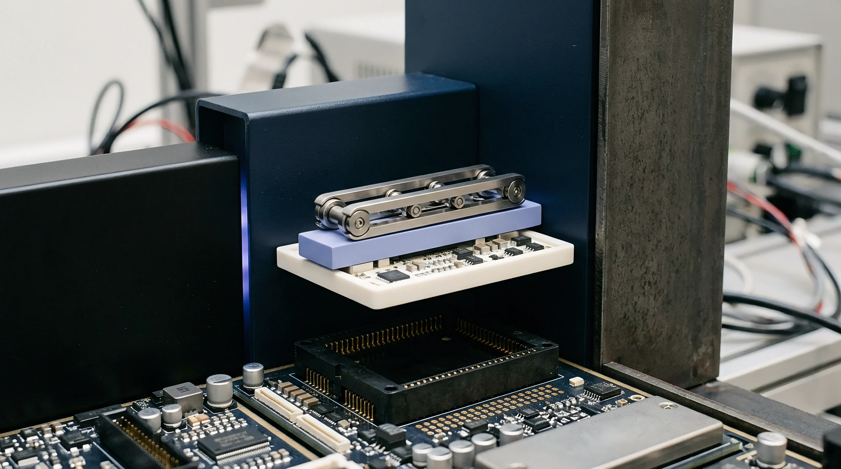
Physical silicon geometry parameters dictate the maximum electric field strength that a package substrate and silicon die stack survive without cumulative dielectric damage.
Matrix
Delta qualification matrices eliminate redundant testing by focusing resources on the hardware subsystems altered during a node transition. Rather than running a full multi-thousand-hour qualification suite under standards like JEDEC JESD47 or AEC-Q100, the engineering team isolates specific change vectors. Constructing an effective matrix requires balancing stress acceleration factors, sample sizes, and risk-weighted failure modes.
The development of a targeted qualification matrix follows a systematic qualification procedure:
- Map every silicon, package, and bill-of-materials modification between the baseline process node and the target node hardware platform.
- Calculate acceleration factors for high-temperature operating life and temperature cycling using updated activation energies matching the advanced silicon physics.
- Establish sample sizes based on standard lot distribution requirements, requiring a minimum of three non-consecutive diffusion lots for core silicon validation.
- Define specific pass and fail threshold parameters for parametric drift, including standby current leakage, clock frequency max limits, and RF transmitter EVM limits.
- Execute environmental, mechanical, and electrical stress sequences while logging parametric drift at predetermined test intervals.
| Stress Test Vector | Standard Reference | Test Parameters & Conditions | Sample Size / Lots | Delta Qualification Justification |
|---|---|---|---|---|
| High Temperature Operating Life (HTOL) | JEDEC JESD22-A108 | 125°C, 1.2x Vdd nominal, 500 Hours | 77 units x 3 lots | Validates BTI and TDDB threshold shift under accelerated electrical field. |
| Temperature Cycling (TC) | JEDEC JESD22-A104 | -40°C to +125°C, 500 Cycles, 2 CPH | 77 units x 1 lot | Verifies thermal expansion compatibility between die, sub-underfill, and package substrate. |
| Highly Accelerated Stress Test (HAST) | JEDEC JESD22-A110 | 110°C, 85% RH, biased, 264 Hours | 25 units x 1 lot | Evaluates moisture ingress and corrosion sensitivity in thinner package passivation layers. |
| Electrostatic Discharge (ESD / LU) | JS-001 / JS-002 | HBM 1.5kV, CDM 250V, Latch-up ±100mA | 6 units / 1 lot | Determines reduced breakdown boundaries on updated sub-micron I/O cells. |
Reduced sample sizes or shortened test durations degrade statistical confidence and increase field escapes. A 500-hour High Temperature Operating Life test at 125 degrees Celsius across 77 units per lot provides statistical coverage equivalent to a 1000-hour baseline run, provided the calculated activation energy reflects advanced gate oxide breakdown physics. The buyer must confirm that the integrator uses activation energies derived from actual advanced node test structures rather than default legacy assumptions.
Section 4.2 of JEDEC JESD47 states that process node changes affecting gate dielectrics or interconnect metallization mandate HTOL and ESD re-evaluation across a minimum of three independent assembly or wafer lots.
Misapplying historical qualification data to a modern node shrink leads to latent field failures, warranty claims, and unscheduled production halts.


Firmware

When Does Process Scaling Invalidate Legacy Register Assumptions?
Hardware abstractions in embedded software often mask underlying silicon characteristics, but node transitions can disrupt driver timing, register access speeds, and physical layer calibration parameters. Advanced node silicon operates at higher internal clock frequencies alongside lower core voltages. Dynamic power management routines written for 28-nanometer silicon may miscalculate phase-locked loop lock times or power domain wake latencies when executed on 16-nanometer FinFET modules.
Physical layer calibration routines rely directly on process-dependent parameters stored in One-Time Programmable (OTP) memory or fuse arrays during factory trimming. Analog-to-digital converters, internal low-dropout regulators, and radio frequency transceivers all depend on these coefficients. When hardware migrates to a smaller node, altered transistor transconductance renders legacy trim formulas inaccurate.
Firmware must parse updated fuse bit maps and execute recalculated formulas to set physical parameters correctly.
Software delay loops introduce major risks during hardware migrations. Legacy register maps break on faster silicon. Firmware relying on cycle-counting loops to generate microsecond delays during peripheral initialization executes much faster on advanced nodes due to improved pipeline efficiency and bus throughput.
These compressed delays cause I2C communication faults, flash write corruption, and power rail stabilization failures. Properly configured hardware abstraction layers prevent these issues by tying delays to dedicated hardware timer peripherals rather than instruction execution loops.
Consider a semi-custom wireless module transitioning from 40-nanometer planar CMOS to 22-nanometer FD-SOI technology. The original driver initialized the onboard low-noise amplifier by writing to control registers, then executed a hardcoded 50-microsecond delay loop before enabling the mixer stage:
On the 40-nanometer platform, the processor core completed the loop in 600 clock cycles at 12 megahertz, matching the required 50-microsecond window. On the 22-nanometer platform, the core runs at 48 megahertz and executes loops more efficiently, finishing the routine in 11.2 microseconds. The mixer enables before the low-noise amplifier bias current stabilizes, creating an impedance mismatch that clips the receiver input stage and drops initial preamble bits.
Resolving this issue requires updating the driver to poll a power management unit hardware status flag rather than relying on software timing.
Treating low-level driver modifications as routine maintenance updates leaves the complete re-verification cycle required for altered physical layer code unaddressed.

Package
A reliable node transition requires a complete design transfer package containing source-level hardware and test artifacts. Receiving only compiled binary images and basic pinout drawings prevents the buyer from performing independent timing, power, or signal integrity analyses. The design transfer package serves as the technical baseline for quality audits, second-source qualification, and regulatory re-certification.
A comprehensive design transfer package for process node hardware transitions must contain specific engineering deliverables:
- Synthesizable RTL Repositories containing Verilog or VHDL source code with full register definitions and hardware abstraction layer driver bindings.
- Calibre DRC Output Logs verifying that layout geometries adhere to updated foundry design rules without unresolved layout-versus-schematic violations.
- ATE Test Vector Sets supplied in STIL or WGL formats, enabling direct execution of wafer-level and package-level production testing on automated test equipment.
- IBIS-AMI Signal Models providing accurate high-speed I/O buffer behavior under varying voltage, temperature, and process corner conditions.
- Thermal Simulation Files detailing package thermal impedance matrices (Theta-JA, Theta-JC) derived from finite element analysis models.
Package redesigns often accompany node migrations to fit smaller die sizes within legacy footprint envelopes. Shrink-ratio differences between the new die and existing package cavity demand underfill adjustments and revised wire-bonding or flip-chip bump layouts. The transfer package must include mechanical Gerber files, substrate layer stackups, and die-attach material data sheets to verify thermal expansion matching between the package substrate and the system printed circuit board.
An engineering transfer package lacks contractual validity unless it contains fully reproducible build scripts, physical design verification logs, and raw automated test equipment vector sets matching the exact silicon stepping.
A standard quality assurance clause in semi-custom supply agreements specifies that any modification to silicon process technology, die size, or package substrate material grants the buyer absolute rights to receive updated GDSII or LEF/DEF layout views alongside revised manufacturing test specifications prior to commercial batch production.

Toll
Process node transitions carry substantial commercial impact driven by Non-Recurring Engineering (NRE) charges, mask tooling amortisation, and yield learning curves. Tooling costs rise steeply on advanced nodes: a 28-nanometer planar mask set costs approximately 750,000 USD, a 16-nanometer FinFET set exceeds 2,500,000 USD, and a 5-nanometer mask set demands over 8,500,000 USD. Tooling costs scale with smaller feature sizes.
These upfront investments must be balanced against per-unit silicon cost savings realized through higher die yield per wafer.
| Integration Level | Initial NRE Cost (USD) | Mask Tooling Ownership | Unit Cost Impact (100k Units) | Yield Risk Allocation |
|---|---|---|---|---|
| Turnkey Module | $50,000 – $150,000 | Retained by Integrator | Baseline + 12% Margin | 100% Integrator Risk |
| Semi-Custom Platform | $450,000 – $1,200,000 | Shared / Co-Owned | 20% Unit Price Reduction | Split via Yield Limits |
| Reference Design Transfer | $1,800,000 – $4,500,000 | Fully Owned by Buyer | 45% Unit Price Reduction | 100% Buyer Risk |
Unit economics shift during the initial ramp of a new node. Raw wafer pricing is considerably higher at advanced geometries; a 300mm wafer at 5-nanometer costs over 16,000 USD compared to 3,000 USD for a 28-nanometer wafer. Net savings only materialize when the die shrinks enough to yield substantially more gross die per wafer, offsetting the premium substrate cost.
Mask sets command massive non-recurring fees. The buyer must pinpoint the break-even production volume where lower unit die costs fully amortize mask NRE and engineering qualification expenses.
Wafer price inflation at advanced nodes negates die-shrink savings unless the active die area drops by at least thirty-five percent relative to the legacy process geometry.
Yield management structures determine which party absorbs scrap losses during early production ramps. Advanced nodes initially show lower defect-free die yields. In turnkey sourcing contracts, the supplier absorbs yield loss but incorporates a risk margin into unit pricing.
In semi-custom and reference design transfer agreements, contracts frequently link unit pricing to wafer yield bands; if defect densities exceed agreed limits, the foundry or integrator issues NRE credits or waives testing fees to offset buyer losses. Foundries share yield risk through wafer limits.
Calculating the true landed cost of a node transition requires tallying NRE fees, unit cost differentials, regulatory re-certification expenses, and firmware development hours. Volume determines the proper commercial approach: lower-volume hardware programs benefit from turnkey arrangements that avoid steep mask charges, while high-volume deployments recover custom tooling investments through reduced per-unit silicon costs across the product lifecycle.