Designing Calibrated Test Fixtures for Automated Lot Verification SOW
A test fixture statement of work must specify pin contact physics, calibration traceability, measurement uncertainty budgets, and native design deliverables.


Probe
Mechanical interface stability dictates the measurement floor in production lot acceptance. When high-volume radio frequency modules or power management integrated circuits enter automated verification, physical contact with test pads introduces parasitic inductance, contact resistance variation, and structural wear that shift measured values away from true device performance. A statement of work for test fixture design requires explicit definitions of pin stroke depth, plating chemistry, contact force profiles, and alignment mechanical tolerances before hardware fabrication begins.
Contract manufacturers frequently use generic pogo pin assemblies that degrade after ten thousand insertions, introducing artificial yield drops that get misdiagnosed as semiconductor lot defects. Specifying calibrated test fixtures demands treating the electromechanical contact point as a precision instrument subject to mechanical wear and electrical calibration limits.
Spring-loaded contacts function as transmission lines at elevated frequencies and as variable resistors under power delivery conditions. Solid gold plating over nickel substrates provides low initial contact resistance, yet abrasive wear against solder-bumped or gold-plated device pads strips the outer gold layer, exposing nickel and copper underplates that oxidize under ambient laboratory humidity. This oxidation increases pin resistance from twenty milliohms to over two ohms within thirty thousand actuation cycles.
Mechanical force profiles must balance wiping action, which breaks surface oxides, against pad deformation that damages device under test substrates. Dual-actuation fixtures apply an initial vertical stroke followed by a micro-wipe motion of fifteen to thirty micrometers, clearing surface films without displacing pad metallization.

Contact Interface Physics and Electrical Degradation
Pin spring force deteriorates through thermal cycling and mechanical fatigue. Beryllium copper and spring steel internal springs lose initial preload force when exposed to repetitive cycling at elevated operational temperatures during burn-in testing. A force drop below fifteen grams per pin results in intermittent electrical contact, high-frequency signal reflection, and false failure reports during automated lot clearance.
Automated fixtures require spring force monitoring or scheduled pin replacement thresholds specified directly within the engineering contract.
| Pin Type | Plating Structure | Initial Contact Resistance | Rated Mechanical Cycles | Current Handling Capacity | Parasitic Inductance |
|---|---|---|---|---|---|
| Standard Spring Probe | Gold over Nickel | 25 mΩ max | 100,000 | 3.0 A | 1.2 nH |
| Kelvin Co-axial Probe | Hard Gold over Palladium-Nickel | 15 mΩ max | 250,000 | 1.5 A (Sense) / 5.0 A (Force) | 0.4 nH |
| High-Frequency RF Socket Pin | Direct Hard Gold | 30 mΩ max | 50,000 | 0.5 A | 0.15 nH |
| High-Current Crown Head Pin | Silver-Nickel Alloy | 8 mΩ max | 150,000 | 10.0 A | 2.1 nH |
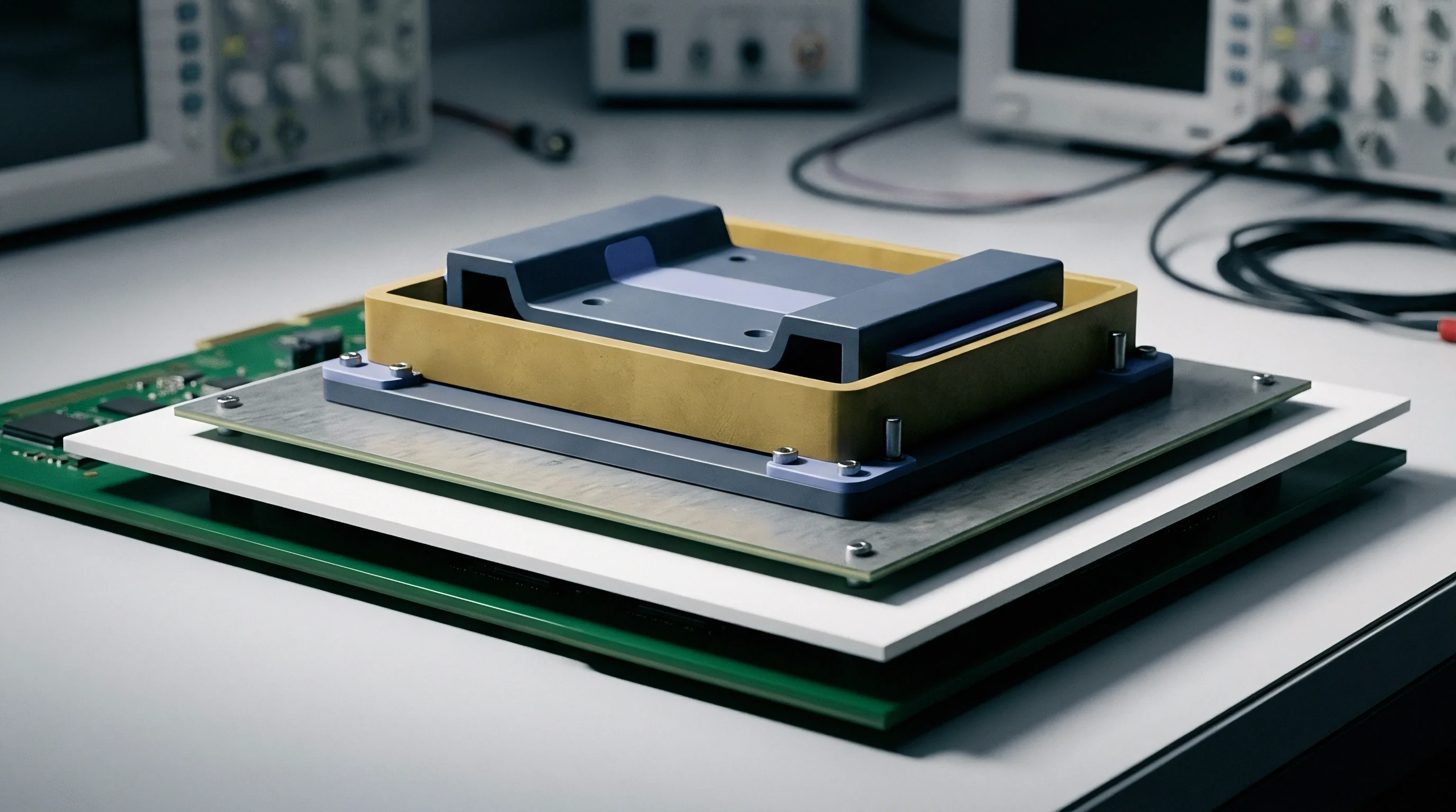
Alignment tolerances between the fixture top plate and the device socket directly control contact reliability. Automated lot handlers position devices within tight spatial bounds, typically plus or minus twenty-five micrometers. Alignment plate drift caused by thermal expansion or guide pin wear introduces lateral shear stress on spring contacts, bending pin plungers and causing mechanical binding inside the barrel.
Top plates fabricated from dimensionally stable glass-epoxy composites or anodized aluminum with hardened steel guide bushings preserve alignment over hundreds of thousands of cycles.
Gold-plated spring probes experiencing fifty thousand mechanical cycles exhibit a fourfold increase in contact resistance when scrub distance exceeds forty micrometers on lead-free solder balls.

Kelvin Four Wire Layouts for High Current Paths
Sense lines routed parallel to high-current force traces introduce measurement errors through magnetic coupling and shared return paths. Four-wire Kelvin contact structures eliminate socket wiring resistance from the measurement loop by separating current delivery lines from voltage sense lines down to the device pad surface. Dual-needle Kelvin probes place two isolated spring plungers inside a single socket cavity, contacting a single test pad with tip separation under zero point three millimeters.
High-current pulse testing induces inductive voltage spikes across fixture trace inductances. Fixture design layouts must minimize loop area between force and return traces to suppress voltage transients during high dI/dt switching tests. Decoupling capacitors placed on the underside of the test fixture interface board, directly beneath the pogo pin socket, reduce parasitic loop inductance below zero point five nanohenries.
This proximity prevents switching transients from corrupting analog measurement channels during automated lot screening.
Shielding radio frequency paths through the fixture interface requires impedance-matched coaxial probe structures or conductive elastomer contact pads. Standard spring probes present an impedance discontinuity at frequencies above one gigahertz, introducing signal attenuation and standing wave ratios that obscure genuine device performance metrics. RF sockets utilizing embedded elastomer matrix conductors surrounded by grounded metal structures maintain a fifty-ohm characteristic impedance up to forty gigahertz, ensuring high-frequency automated lot clearance remains accurate across production runs.
When contact degradation causes unexpected yield drops, the loss is frequently mistaken for defective metal pads on the semiconductor wafer lot.


Calibration
Reference standards establish the metrological baseline for every automated lot verification suite. Without a verified chain of measurements extending to national standards institutes, test fixtures generate data that fails regulatory audits and customer acceptance checks. Calibrated test fixtures rely on specialized artifact boards containing high-precision, low-temperature-coefficient passive components and short-open-load-thru networks.
These artifact boards pass through the fixture alignment mechanism under identical mechanical constraints as production device lots, mapping fixture signal path losses, DC offsets, and switching delays.
Secondary reference boards deteriorate through physical handling, thermal exposure, and component aging. Using production units as reference standards introduces unquantified drift into the lot acceptance pipeline. Master calibration artifacts utilize ceramic substrates with thin-film resistor networks exhibiting temperature coefficients under five parts per million per degree Celsius.
Storing calibration artifacts in temperature-controlled enclosures preserves their reference values over extended operational periods.

Metrological Traceability to National Standards
Primary voltage references certified under ISO/IEC 17025 anchor the automated instrument rack supporting the test fixture. The statement of work must define the calibration hierarchy, detailing how reference instruments inside the automated test station map their measurement uncertainties to national standard references. Secondary transfer standards, mounted directly onto calibration interface cards, execute automated routine checks prior to every production lot run.
If a routine check reveals drift exceeding pre-set guardband limits, the test executive halts production and prompts operator recalibration.
Thermal gradients within test enclosures create thermoelectric EMF voltages across dissimilar metal junctions in the signal path. Copper-to-beryllium-copper junctions generate up to nine microvolts per degree Celsius temperature differential. In low-voltage measurement applications, such as microvolt-level sensor interface verification, these thermal EMF voltages corrupt lot data.
Automated calibration routines correct for thermal EMF by performing dual-polarity measurement cycles or applying thermal zero-offset compensation prior to executing active lot tests.

Automated Self Calibration Routines and Drift Triggers
Internal relay networks connect high-precision reference standards to measurement instrument channels during automated self-calibration cycles. Scheduled self-calibration runs between lot batches verify switching matrix paths, trace resistance, and analog-to-digital converter linearity without requiring human intervention or physical disassembly of the test fixture. Automated self-calibration detects relay contact pitting, cable strain failures, and amplifier drift before defective units enter customer supply chains.
Fixture drift metrics define when automated testing must pause for physical inspection and maintenance. System software tracks key calibration parameters across consecutive lot runs, analyzing drift velocity and statistical variance.
Self-calibration routines execute short-open-load-thru algorithms at the pogo pin contact plane using specialized calibration plates. Open standards clear stray capacitance, short standards cancel loop resistance and inductance, and load standards normalize frequency response across measurement bands. Implementing these routines at the fixture interface level moves the reference plane directly to the device contact point, eliminating cable loss and fixture trace distortion from final test results.
Section 8.2 of ISO 17025 contracts requires measuring equipment to be calibrated across its full operational range before initial release to production lot verification.
The statement of work establishes that any lot verified while a test fixture operates outside its documented calibration window is subject to mandatory re-testing at the fixture integrator’s sole expense.


Automation
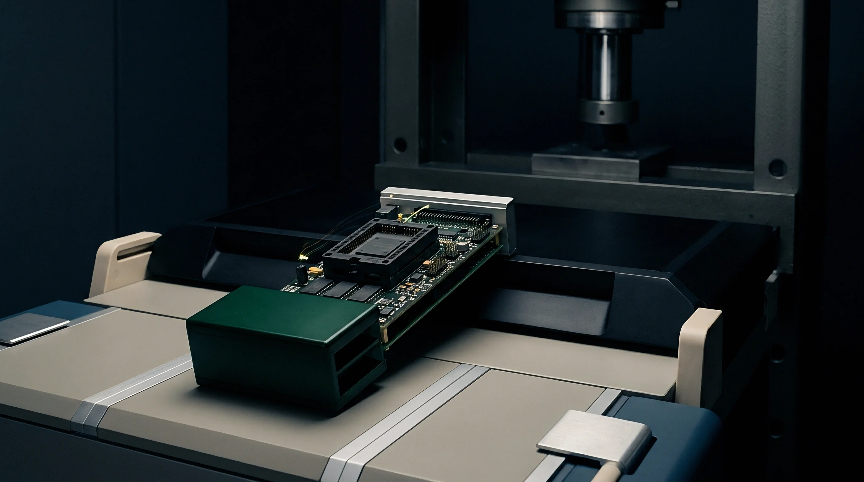
Instrument multiplexing increases test station throughput by routing expensive instrumentation across multiple test sockets. Automated lot verification systems rely on switching matrices composed of electromechanical relays, reed relays, or solid-state switches to route high-frequency, high-current, and sensitive analog signals between the device under test and measurement hardware. Fixture designers must evaluate switch settling times, contact bounce characteristics, isolation resistance, and bandwidth performance when building automated multiplexing circuits into the test interface board.
Electromechanical relays handle high current loads and provide low contact resistance, but their slow actuation times, typically five to fifteen milliseconds, constrain test speed. Reed relays offer faster actuation, between zero point two and one millisecond, with low contact parasitics, making them suitable for fast analog multiplexing. Solid-state switches deliver microsecond switching speeds and infinite mechanical lifespan, but introduce non-linear series resistance and parasitic capacitance that distort high-frequency and low-current measurements.
Switching Matrix Architecture and Signal Isolation
Crosstalk between adjacent measurement channels corrupts lot verification data during multi-site parallel testing. High-density switching matrices require guard traces and ground shielding between signal paths to prevent capacitive and inductive coupling. Driven guard shields, held at the same electrical potential as the high-impedance sense line, eliminate leakage currents through PCB insulation resistance and suppress high-frequency noise pickup from adjacent switching channels.
| Switch Topology | Actuation Speed | Contact Resistance | Channel Isolation at 1 GHz | Lifespan (Cycles) | Thermal EMF |
|---|---|---|---|---|---|
| Electromechanical Armature | 10.0 ms | 50 mΩ | -45 dB | 5,000,000 | < 5 µV |
| Hermetic Reed Relay | 0.5 ms | 100 mΩ | -60 dB | 100,000,000 | < 20 µV |
| Solid-State CMOS Switch | 0.005 ms | 2.5 Ω | -30 dB | Infinite | 0 µV |
| MEMS RF Switch | 0.010 ms | 1.2 Ω | -65 dB | 1,000,000,000 | < 2 µV |
Tree-structured matrix topologies reduce parasitic capacitance compared to simple crossbar arrays by disconnecting unused stub lines from the active measurement path. Stub traces act as quarter-wave transmission line resonators at specific frequencies, creating deep notch filters that attenuate test signals. Fixture layout design must keep stub lengths below one-twentieth of the wavelength of the highest test frequency to maintain signal integrity.
Control Loop Latency and Executive Test Software
Executive test suites manage instrument drivers, relay control, and data logging through hardware-synchronized trigger buses. Software-driven polling of instrument status registers introduces non-deterministic delays ranging from two to fifty milliseconds per test step, bloating lot test execution times. Hardware triggering via dedicated digital I/O lines synchronizes relay state changes, power supply stepping, and digitizer capture sequences down to microsecond boundaries, maximizing automated lot clearance velocity.
Industrial communications protocols between the test host and the fixture control board utilize isolated Ethernet or USB interfaces to prevent ground loops. Isolation barrier breakdown voltage specifications must exceed two thousand volts DC to protect sensitive measurement instruments from high-voltage transients during device failure modes. Embedded microcontrollers on the fixture interface board execute localized control loops, performing high-speed continuity checks before connecting sensitive measurement channels to the device under test.
Safety interlock circuits integrated into the fixture housing prevent operator exposure to high voltages and protect internal components from mechanical damage during handler operation. Pneumatic actuators driving the fixture clamp assembly incorporate optical position sensors and pressure transducers, preventing actuation if a device sits improperly aligned inside the contact socket. Interrupt-driven firmware immediately opens safety relays and halts handler movement upon detecting an interlock breach.
Switch actuation settling times must elapse completely before analog-to-digital converter triggering begins to avoid measuring transient relay bounce voltages.
Designing matrix routing paths with short, symmetrical trace geometries prevents phase distortion across multi-channel parallel test interfaces.

Uncertainty
Statistical variance in automated testing arises from instrument accuracy, fixture contact resistance, environmental temperature swings, and software calculation tolerances. Establishing a comprehensive measurement uncertainty budget per the ISO/IEC Guide to the Expression of Uncertainty in Measurement (GUM) allows engineering teams to calculate expanded uncertainty values with defined confidence intervals. High uncertainty budgets force test limits inward, causing false rejection of acceptable production lots and increasing scrap costs for the manufacturer.
Gage Repeatability and Reproducibility (Gage R&R) studies quantify the fraction of total test variance contributed by the measurement system itself versus true product variation. A Gage R&R result below ten percent demonstrates an acceptable measurement system, while values above thirty percent indicate that the test fixture and instrument chain cannot reliably sort good devices from bad devices. Statement of work provisions must mandate acceptable Gage R&R thresholds across all critical-to-quality lot verification parameters before final fixture commissioning.

Measurement System Analysis and Gage Calibration Ratios
Repeatability and reproducibility studies isolate fixture mechanical instabilities from instrument drift. Operators or automated handlers load identical reference samples into the fixture across multiple evaluation passes, logging parameter values to separate mechanical contact variation from instrument noise floor. If contact variation dominates total uncertainty, the fixture mechanical clamp, pogo pin selection, or top plate alignment guide requires redesign.
Test capability index metrics evaluate fixture precision against specified engineering tolerances. Maintaining a high test capability ratio requires instrument measurement uncertainty to remain a small fraction of the overall product specification width. Fixtures designed with insufficient guardbanding fail to detect marginal defect states, allowing non-conforming product lots to escape to downstream assembly lines.
- Assemble a dedicated sample set of ten devices representing the full process variation spectrum of the production line.
- Calibrate the automated test station instrumentation using primary traceable reference standards.
- Execute five consecutive automated test passes per device without removing the units to establish pure instrument repeatability variance.
- Remove and reload each device ten distinct times using the automated handler to measure fixture mechanical contact reproducibility variance.
- Calculate the combined standard uncertainty using root-sum-square summation of all identified Type A statistical variances and Type B systematic uncertainties.
- Derive the expanded uncertainty using a coverage factor of k equals two, corresponding to a ninety-five point four five percent confidence interval.
- Apply the calculated expanded uncertainty as an internal guardband subtractor against upper and lower customer product specification limits.
Which Guardband Multiplier Minimizes False Lot Rejection?
Tightening test limits protects downstream assembly lines from receiving out-of-spec components, but aggressively wide guardbands cause severe yield loss on conforming manufacturing lots. Setting guardband widths equal to one times the expanded measurement uncertainty reduces the risk of accepting a non-conforming device below zero point one percent, assuming a normal distribution of product attributes. Choosing the optimal guardband multiplier involves balancing the financial penalty of false lot rejections against the commercial liability of shipping defective products to end customers.
| Guardband Multiplier | Effective Test Limit Width (% of Spec) | Consumer Risk (False Accept Rate) | Producer Risk (False Reject Rate) | Impact on Manufacturing Lot Scrap Cost |
|---|---|---|---|---|
| 0.0 (No Guardband) | 100.0% | 2.270% | 0.000% | Baseline Scrap Rate |
| 0.5 × Expanded Uncertainty | 95.0% | 0.620% | 0.350% | + 0.8% Yield Loss |
| 1.0 × Expanded Uncertainty | 90.0% | 0.035% | 1.850% | + 3.2% Yield Loss |
| 1.5 × Expanded Uncertainty | 85.0% | 0.001% | 4.900% | + 8.5% Yield Loss |
| 2.0 × Expanded Uncertainty | 80.0% | < 0.0001% | 9.300% | + 16.2% Yield Loss |
Type A uncertainties are evaluated through statistical analysis of series of observations, capturing random noise, thermal drift, and mechanical positioning jitter. Type B uncertainties are derived from instrument manufacturer specifications, calibration certificate uncertainties, and thermal coefficients. Combining Type A and Type B uncertainties via the law of propagation of uncertainty accounts for cross-correlation terms between measurement channels, preventing underestimation of total measurement error.
Guardbanding calculations must incorporate environmental temperature drift inside factory operational floors. A test fixture calibrated at twenty-two degrees Celsius that operates inside an automated handler enclosure at forty-five degrees Celsius suffers from drift caused by thermal expansion of mechanical components and temperature coefficients of signal conditioning passives. Enclosure climate control systems or real-time temperature compensation software routines reduce environmental uncertainty components within the lot verification budget.
Failing to account for parasitic resistance drift in high-current test paths understates measurement uncertainty, leading to unverified yield drops that cost semiconductor vendors tens of thousands of dollars per scrapped lot.

Dossier
Complete engineering transfers require comprehensive documentation packages delivered alongside physical test fixture hardware. A statement of work for test fixture design must detail all required electronic design interchange files, fabrication outputs, mechanical CAD assemblies, firmware source code repositories, and calibration procedures. Accepting a test fixture without acquiring native design files locks the buyer into a single vendor for future fixture maintenance, modifications, and second-sourcing initiatives.
Proprietary design file formats prevent seamless integration with downstream manufacturing execution systems and secondary engineering suppliers. Native CAD files created in industry-standard tools, alongside neutral export formats such as STEP for 3D mechanical models and IPC-2581 for printed circuit board fabrication, must accompany every physical shipment. Complete file deliveries empower receiving factories to manufacture identical secondary fixtures during production scaling phases.
Fabrication Outputs and Hardware Transfer Packages
Schematics, bill of materials documents, and PCB layout files represent the core hardware documentation package. The statement of work must mandate open disclosure of all component part numbers, including custom machined housings, spring probe model codes, matrix relay references, and connector pinouts. Generic or anonymized part entries inside bill of materials spreadsheets prevent timely fixture repair when components fail on active production lines.
Firmware compiled onto localized fixture control boards demands source code delivery, build environment documentation, and version control repository access. Embedded code executing on microcontrollers manages relay sequencing, safety interlocks, and calibration constant storage. Delivery packages must include unencrypted C/C++ source code, toolchain installation scripts, register maps, and compiled binary images to enable independent code audits and future enhancements.

Acceptance Protocols for Factory and Site Signoff
Factory Acceptance Testing (FAT) validates fixture mechanical operation, electrical continuity, and measurement noise performance at the supplier’s development facility prior to shipping. Site Acceptance Testing (SAT) verifies fixture integration with the customer’s handler, instrumentation rack, and production software executive inside the destination manufacturing plant. Passing FAT criteria does not guarantee passing SAT, as environmental noise, line voltage variations, and handler mechanical interfaces introduce operational variables.
Acceptance protocols must include running a standardized verification lot of known good and known bad devices through the fixture interface. Passing criteria demand one hundred percent correct classification of conforming and non-conforming devices across three consecutive runs without mechanical jam or communication error. Final commercial payment milestones remain tied to formal SAT customer signoff documentation.
Delivery of uncompiled source code, raw Gerber packages, and native mechanical design files serves as a mandatory prerequisite for final SOW invoice settlement.
What technical remediation mechanisms apply if a delivered test fixture passes supplier Factory Acceptance Testing but fails operational Site Acceptance Testing due to uncharacterized electrical noise in the buyer’s factory environment?

Amortization
Commercial structures for test fixture procurement separate upfront Non-Recurring Engineering (NRE) charges from recurring per-unit manufacturing costs and wear-and-tear component replacement schedules. An explicit scope of work details hourly engineering rates, custom tooling expenses, material costs, and intellectual property ownership rules before design execution starts. Unclear scope descriptions often result in unexpected billing additions when fixture modifications become necessary during final system integration.
Engineering charges itemized across custom PCB layout, mechanical housing design, firmware development, and metrological validation prevent suppliers from masking inflated margins inside lump-sum quotation line items. Clear financial breakdowns allow procurement teams to benchmark development expenses against market averages and negotiate volume-based discounts for secondary fixture builds.
Non Recurring Engineering Breakdown and Ownership Mechanics
Intellectual property ownership clauses inside the scope of work determine whether the buyer or the fixture integrator owns custom circuitry, specialized probe layout techniques, and embedded firmware architecture. Work-for-hire agreements vest full IP rights, design patents, and file custody in the purchasing entity, enabling unrestricted transfer of fixture designs to third-party manufacturing plants. Retaining joint IP ownership may reduce initial NRE charges, but limits the buyer’s long-term sourcing flexibility.
Tooling charges cover specialized machining jigs, drill plates, injection molds, and alignment fixtures required to manufacture pogo pin blocks and interface enclosures. The statement of work must specify that all physical tooling funded through NRE payments remains the exclusive physical property of the buyer, held in bailment by the supplier. Provisions for tool retrieval or transfer upon contract termination protect the buyer against supplier lock-in.

Per Unit Tooling Recovery and Wear Maintenance Schedules
Tooling replacement costs scale directly with production batch volume and physical fixture wear limits. High-volume automated lot verification lines require scheduled replacement of wearable sub-assemblies, specifically pogo pin plates, alignment bushings, and switching relays. Contract terms define whether wear-and-tear component maintenance is billed per service event or amortized into a fixed per-unit test fee charged against each verified production module.
Amortizing NRE costs into per-unit module testing fees introduces commercial risks if production volumes fall below forecast targets. If lot volumes undershoot estimates, the fixture supplier fails to recover development expenses, while volume overshoots result in overpayment by the buyer. Direct upfront payment of NRE fees combined with cost-of-goods pricing for duplicate fixtures creates a transparent financial structure aligned with actual production outcomes.
Maintenance schedules tied to total contact insertion counters prevent unexpected line downtime during lot runs. Automated test software logs every handler clamp cycle, alerting operators when spring probes approach eighty percent of their rated mechanical lifespan. Replacing wearable contact blocks during scheduled maintenance windows avoids mid-run fixture failures that corrupt test data and stall lot verification pipelines.
Fixture procurement contracts should be structured to include explicit spares kits containing pre-calibrated probe plates, replacement relays, and guide bushings delivered alongside primary hardware. Having validated replacement assemblies on site minimizes mean time to repair, ensuring automated lot verification throughput remains uninterrupted throughout the product lifecycle.