Micro Asperity Deformation Mechanics and Oxide Film Penetration in Automated Socket Interfaces
Micro-asperity deformation and mechanical wipe breach insulating surface oxides to preserve low socket contact resistance during peak radio transmit bursts.

Contact
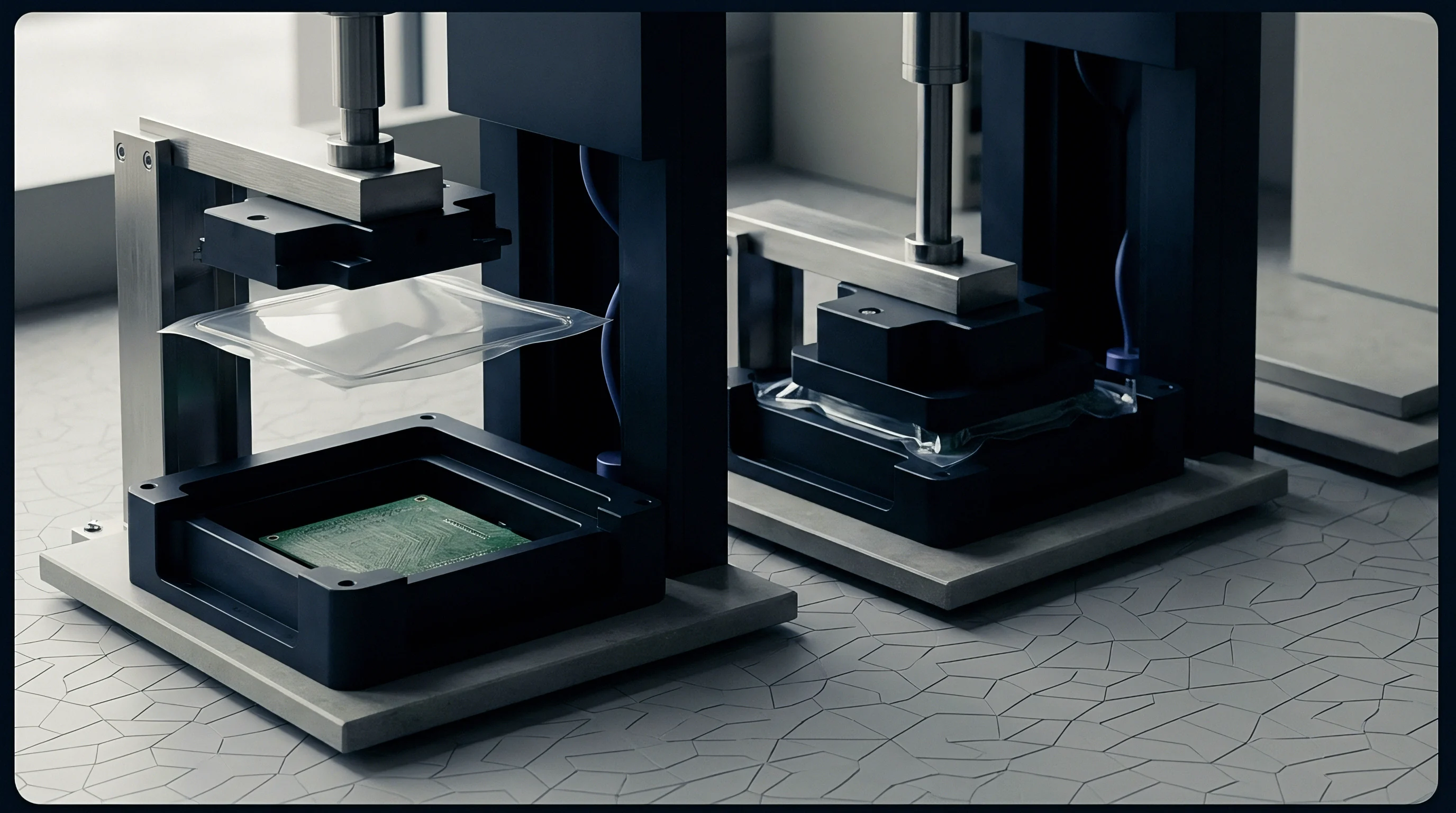
Even polished contacts and gold-plated pads are rough under magnification, covered in microscopic peaks and valleys called asperities. When an automated test fixture seats a module into a socket, physical contact happens only at those high points. As a result, the nominal contact area derived from pogo pin tip geometry is misleading; under standard actuation forces, true metallic contact is confined to the flattened tips of mating asperities, which occupy less than one percent of the apparent contact region.
Applying normal force concentrates high localized stress at these contact points. The initial engagement is elastic, but as the load climbs past the yield strength of the softer pad metal, plastic deformation takes over. The asperities flatten out, widening the real contact area and bringing conductive sub-layers together.
On copper pads finished with immersion gold, the yield strength of the underlying nickel sets this plastic threshold, dictating the minimum normal force per pin needed to establish low-resistance metal-to-metal bridges.
Mechanical wipe displaces non conductive tin oxides from the electrical contact zone into peripheral troughs.
Constriction resistance develops because current lines are forced through these isolated micro-asperity junctions. When current travels through a pogo pin, it funnels through tiny metallic bridges, generating a localized voltage drop even on clean surfaces. Under Maxwell constriction theory, this resistance is inversely proportional to the sum of the contact-spot radii.
Adding mechanical load broadens existing spots and creates new contact points, lowering constriction resistance along a non-linear curve until the interface reaches plastic saturation.
| Pad Surface Finish | Hardness (HV) | Yield Stress (MPa) | Elastic Modulus (GPa) | Threshold Force (cN) |
|---|---|---|---|---|
| Electroless Nickel Immersion Gold | 350 to 500 | 1200 | 200 | 12.5 |
| Hard Gold over Nickel | 150 to 220 | 600 | 110 | 8.0 |
| Immersion Tin | 12 to 20 | 50 | 50 | 2.5 |
| Hot Air Solder Leveling | 15 to 25 | 60 | 48 | 3.0 |
Over millions of test cycles, spring relaxation upsets this balance. Internal springs lose force under continuous thermal and mechanical stress, reducing the peak force delivered at full compression stroke. If normal force falls below the level required to maintain plastic deformation at the asperities, the real contact area contracts.
The resulting surge in current density across the remaining spots drives localized Joule heating, which accelerates oxidation and mechanical fretting wear on the automated socket interface pins.

Foil
Exposed to factory air, metallic test pads develop insulating surface films within hours. Copper oxidizes into cuprous oxide and cupric oxide layers, while tin builds a dense passivating film of stannic oxide. Gold-plated test pads are not immune either: underlying nickel or copper diffuses through thin gold porous channels to create surface oxide film layers.
During automated socketing, these dielectric films obstruct test signals, turning direct metallic junctions into complex metal-insulator-metal structures.
Breaching these surface oxides takes a combination of mechanical and electrical forces. Under pure normal load, hard thin oxides resist plastic deformation by distributing stress into the underlying softer bulk metal, causing the oxide film to flex without fracturing. A thin film acts like a flexible skin over a soft core.
Pervasive oxide films require a critical shear strain to crack open, exposing pristine, unoxidized metal beneath the fractured surface layer.
When mechanical contact does not fully fracture the oxide film, fritting provides a secondary electrical path. If the voltage applied across an insulating oxide layer exceeds its dielectric breakdown threshold, an intense localized electric field forms. Field strength reaching one million volts per centimeter breaks down the insulating lattice.
Metal atoms drift into the ruptured dielectric zone, creating narrow conductive filaments known as A-fritting bridges that restore electrical conductivity through the oxide film.
- Cohesive oxide shear failure occurs when high lateral mechanical shear forces exceed the internal tensile strength of the surface oxide scale, fracturing the oxide layer into discrete microscopic plates.
- Substrate displacement cracking happens as soft bulk solder or tin beneath a rigid oxide layer undergoes plastic flow, leaving the unsupported surface film to crack under vertical pogo tip penetration.
- Dielectric field breakdown initiates when localized bias voltages across unpunctured oxide films create current discharge channels, fusing micro-asperity points without mechanical contact.
- Fretting corrosion buildup develops when small-amplitude mechanical vibrations shift contact spots repeatedly, continually exposing fresh metal that oxidizes and traps insulating debris inside the interface.
Fritting requires voltages that exceed typical low-level signal testing limits. Open-circuit voltages in automated dry-circuit resistance measurements are deliberately capped below twenty millivolts to prevent artificial fritting breakdown. Because of that restriction, intermittent test failures often trace back to unpunctured surface film resistance on the test pads rather than external bench noise.
Scrub
Automated sockets rely on controlled wiping action to clear passivating oxides from module pads. Wiping mechanics translate the vertical downward force of the automated test head into a horizontal sliding motion across the test pad surface. As the pogo pin or cantilever contact depresses, the probe tip travels along a predefined arc, dragging its sharp profile across the metallized landing area.
This lateral scrub motion cuts through surface contamination, pushing fractured oxide debris ahead of the contact edge.
A normal force of 0.15 newtons per pogo pin limits contact resistance to under 20 milliohms across 50000 automated insertions on immersion gold test pads.
Tip geometry governs the shear stress applied to the surface film layer. Spear-point and chisel-point tip geometries concentrate vertical force onto a narrow edge, creating localized contact pressures that slice cleanly through hard nickel and aluminum oxides. Crown-tip contacts distribute normal load across four or four sharp points, offering redundant contact paths at the expense of reduced per-point oxide penetration depth.
Cantilever pins provide longer scrub lengths but require wider pad clearances to accommodate horizontal tip travel without shorting adjacent pins.
- Mount the high-speed optical alignment camera directly above the empty automated socket frame.
- Actuate the robotic placement head to compress a mechanical gold-standard calibration module into the socket at nominal test height.
- Measure lateral tip deflection across thirty representative contact pins using calibrated vision analysis software.
- Record total horizontal scrub distance along the pad surface plane to confirm compliance with minimum oxide displacement tolerances.
- Verify scrub mark depth using three-dimensional laser profilometry on target test pads post-actuation.
Too much scrub movement damages thin-film surface platings, wearing through immersion gold layers down to the nickel barrier in under ten thousand automated socket cycles. Once base nickel is exposed to open factory air, rapid oxidation increases contact resistance exponentially. Optimal socket design balances scrub distance against tip geometry, creating just enough mechanical shear to displace oxides without scoring the base copper laminate beneath the pad finish.
Accurate mechanical alignment keeps the probe tip from skidding outside designated pad boundaries during automated high-volume testing.
Drop
Contact resistance instability directly disrupts radio performance testing during automated wireless module verification. Wireless protocols like LTE-M, NB-IoT, and Wi-Fi 6 generate heavy current pulses during transmit activity. When a cellular module ramps its power amplifier to deliver a 23 dBm RF burst, peak current draw spikes from a few microamperes up to two amperes in under ten microseconds.
Any stray resistance at the socket interface causes an instantaneous drop in supply voltage delivered to the module power rails.
Dynamic voltage drops across high-resistance pogo pins frequently trigger low-voltage lockout circuits on the device under test. A module operating near its lower supply limit of 3.3 volts will reset if contact resistance introduces a supply drop exceeding two hundred millivolts during a transmit pulse. This issue mimics firmware crashes or defective silicon on the production line, causing functional yield loss despite perfectly healthy wireless hardware.

Why Does Mechanical Asperity Decay Degrade RF Link Verification?
RF interface pins present distinct electrical challenges compared to low-frequency supply lines. At 2.4 GHz, 5.8 GHz, and sub-GHz wireless bands, a pogo pin acts as a stub transmission line with parasitic inductance and micro-asperity film capacitance. Oxidized micro-asperity contacts create non-linear contact impedance, altering the return loss and insertion loss profiles of the test interface.
Impedance mismatches reflect RF energy back into the transmitter output stage, degrading measured error vector magnitude and power output accuracy on automated test benches.
| Protocol Standard | Peak Current (mA) | Pulse Width (ms) | Target Voltage (V) | Max Contact Resistance (mΩ) |
|---|---|---|---|---|
| LTE-M Band 20 (23 dBm) | 650 | 0.575 | 3.60 | 45 |
| NB-IoT Standalone (23 dBm) | 420 | 10.000 | 3.30 | 50 |
| Wi-Fi 6 IEEE 802.11ax (20 dBm) | 850 | 2.100 | 3.30 | 30 |
| Bluetooth LE 5.4 (8 dBm) | 35 | 0.300 | 3.00 | 250 |
| LoRaWAN SX1262 (22 dBm) | 120 | 50.000 | 3.30 | 120 |
High contact resistance also converts peak RF energy into heat directly at the socket contact points. Intermittent micro-asperity arcs occurring during high-power wireless transmissions accelerate localized oxidation, increasing film thickness and exacerbating electrical noise. A multi-protocol test line requires precise contact resistance monitoring to avoid misclassifying good radio hardware as failing output power specifications.
Matching probe tip profiles to pad metallurgy prevents early interface wear and reduces transient voltage sag events during automated screening.
Evaluating socket designs involves balancing probe force against pad life:
- Spear tip contacts pierce hard nickel passivated layers effectively, maintaining low contact resistance on electroless nickel immersion gold pads over long screening runs.
- Chisel tip configurations cut through heavy tin oxide films on immersion tin surfaces, providing low electrical resistance across wide high-power supply pads.
- Four-point crown designs provide parallel current paths across soft gold pads, reducing current density per point during high-power Wi-Fi and cellular transmit pulses.
- Flat elastomeric contacts minimize physical mark depth on delicate soft-gold RF pads, preserving surface integrity for secondary assembly steps.
EIA 364 23 specifies dry circuit contact resistance testing below 20 millivolts to ensure oxide films are not electrically punctured during measurement.
Failing to account for transient voltage drops during high-current protocol bursts leads directly to artificial module rejections, unnecessary socket replacement cycles, and corrupted RF calibration data across production batches.
Margin
Contact lifecycle degradation introduces financial risk into cross-border module sourcing operations. Socket interfaces are consumable items with finite operational spans, typically specified for fifty thousand to five hundred thousand insertions under lab conditions. In high-volume automated manufacturing environments, atmospheric sulfur, humidity, and microscopic pad debris drop actual socket lifetime well below vendor claims.
Unplanned socket degradation distorts production yield statistics, driving up landed costs per tested module.
Calculating the true cost of socket ownership requires accounting for both hardware costs and re-test labor caused by intermittent oxide contacts. When an automated test socket degrades, contact resistance instability creates false failure reports during automated firmware flashing and RF power sweeps. Retesting false failures consumes valuable automated test equipment machine hours, slowing down total factory throughput and delaying module delivery schedules.
Automated screening lines implement statistical process control tracking to catch micro-asperity degradation before yield crashes occur. By monitoring average power-rail voltage drop and tracking re-test rates on a per-socket basis, quality control teams identify worn or oxidized pogo pins before contact resistance spikes compromise calibration integrity. Scheduled cleaning cycles using ultrasonic baths or mechanical scrub plates restore contaminated tips, extending socket service life.
Procurement specifications for automated test fixtures require explicit performance metrics that bind suppliers to measured contact resistance limits under real operating duty cycles. Sourcing documentation must define maximum allowable resistance drift, minimum tip wipe distances, and specific pad plating compatibility rules rather than relying on standard vendor lifespan estimates.
A comprehensive procurement agreement incorporates standard clause provisions covering interface contact reliability under automated operational conditions:
Sharp chisel probes pierce thick passivated oxides cleanly but accelerate pad cratering during high volume robotic testing.
Legal specification clauses mandate that socket vendors verify pin contact resistance below thirty milliohms across fifty thousand continuous insertions under specified factory humidity limits, shifting financial liability for premature socket oxide failures directly back to the interface supplier.