Electromagnetic Field Discontinuity and Skin Depth Anomalies across Plastically Deformed Asperity Junctions at Hundred Gigahertz Frequencies
Plastic deformation at 100 GHz contact asperities expands effective skin depth and adds up to 1.8 dB flange loss, collapsing sub-THz radio link margins.
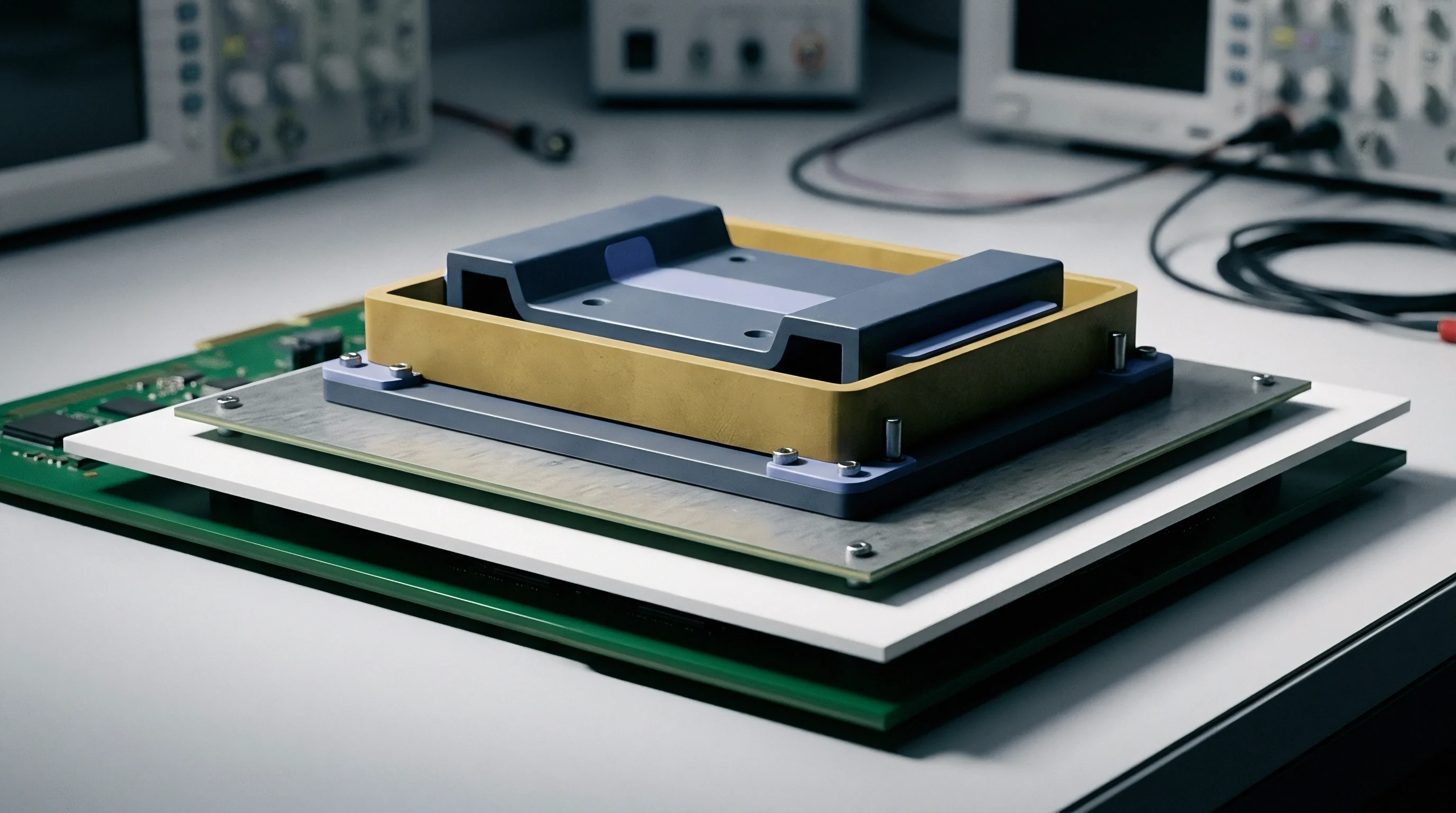

Ridge
Mechanical contact between metallic conductor faces across sub-terahertz transceivers relies on micro-scale surface interactions. When waveguide flanges, coaxial connectors, or flip-chip bumps are mated, contact does not occur across the continuous nominal surface area. Real physical contact is confined to microscopic peaks known as asperities.
The total real contact area represents less than two percent of the geometric contact area under standard mounting forces.
Clamping pressure concentrated on these tiny contact points creates localized stresses that easily exceed the yield strength of common RF conductor metals. Annealed copper exhibits a micro-yield strength near 70 MPa, while gold plater layers yield at 100 MPa to 150 MPa. As clamping force scales, asperities experience severe plastic deformation.
Metal yields under pressure.
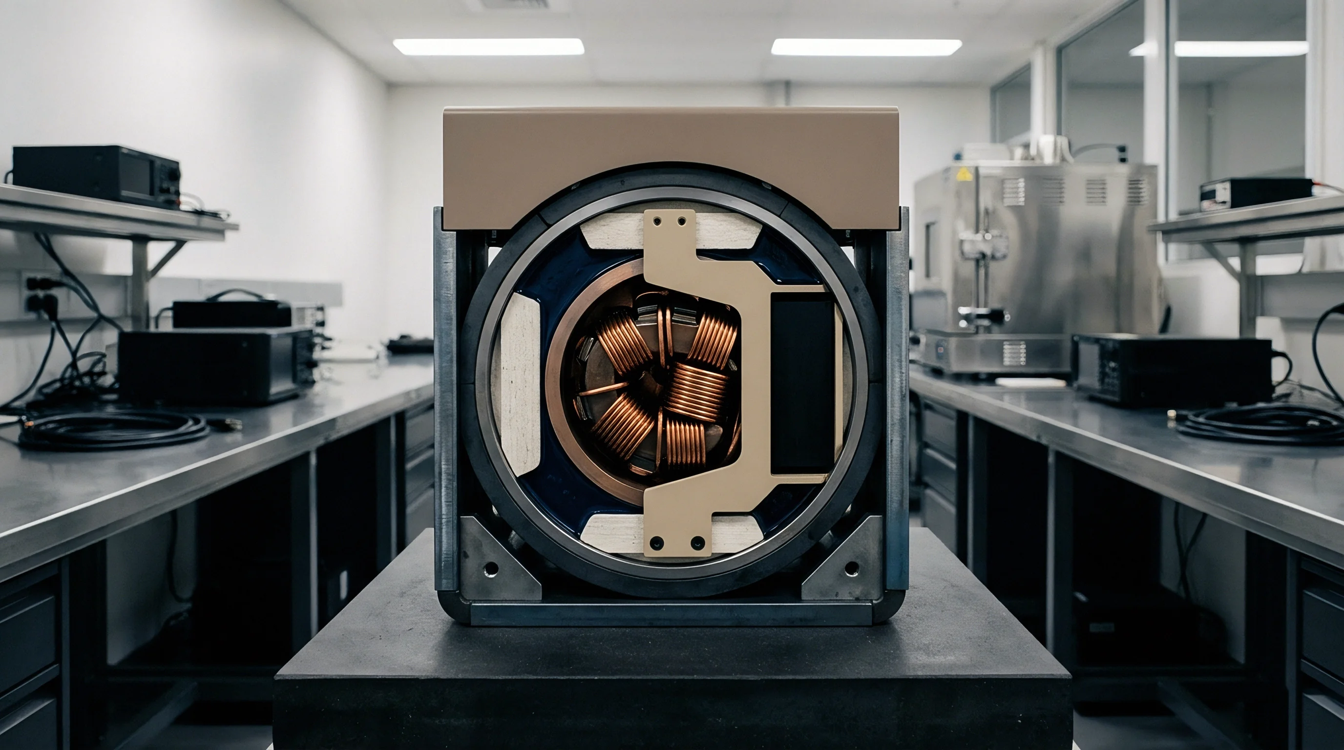
Asperity Yield Behavior under Mechanical Clamping
Plastic deformation flattens microscopic peaks, altering the mechanical profile of the interface. This material flow is not benign to high-frequency current flow. The severe lattice distortion during plastic yield generates dense networks of dislocation lines inside the crystal structure.
Pristine annealed copper contains a dislocation density of approximately 106 cm-2, whereas plastically deformed asperity junctions show dislocation densities exceeding 1011 cm-2.
At a operating frequency of 100 GHz, electromagnetic waves propagate along a shallow conductor region defined by skin depth. The nominal classical skin depth for pure copper with a conductivity of 5.8 x 10⁷ S/m is calculated as:
δ = sqrtfrac2ω μ0 σ
Skin depth shrinks rapidly.
At 100 GHz, this nominal skin depth measures approximately 209 nm. For gold coatings with a conductivity of 4.1 x 10⁷ S/m, skin depth drops to 248 nm. Because the plastic deformation zone beneath crushed asperities extends 100 nm to 500 nm deep, the entire electromagnetic current flows through heavily work-hardened material filled with crystal defects.
At 100 GHz, copper skin depth measures 209 nm while the plastic deformation zone under 150 MPa contact pressure penetrates 350 nm into the surface lattice.
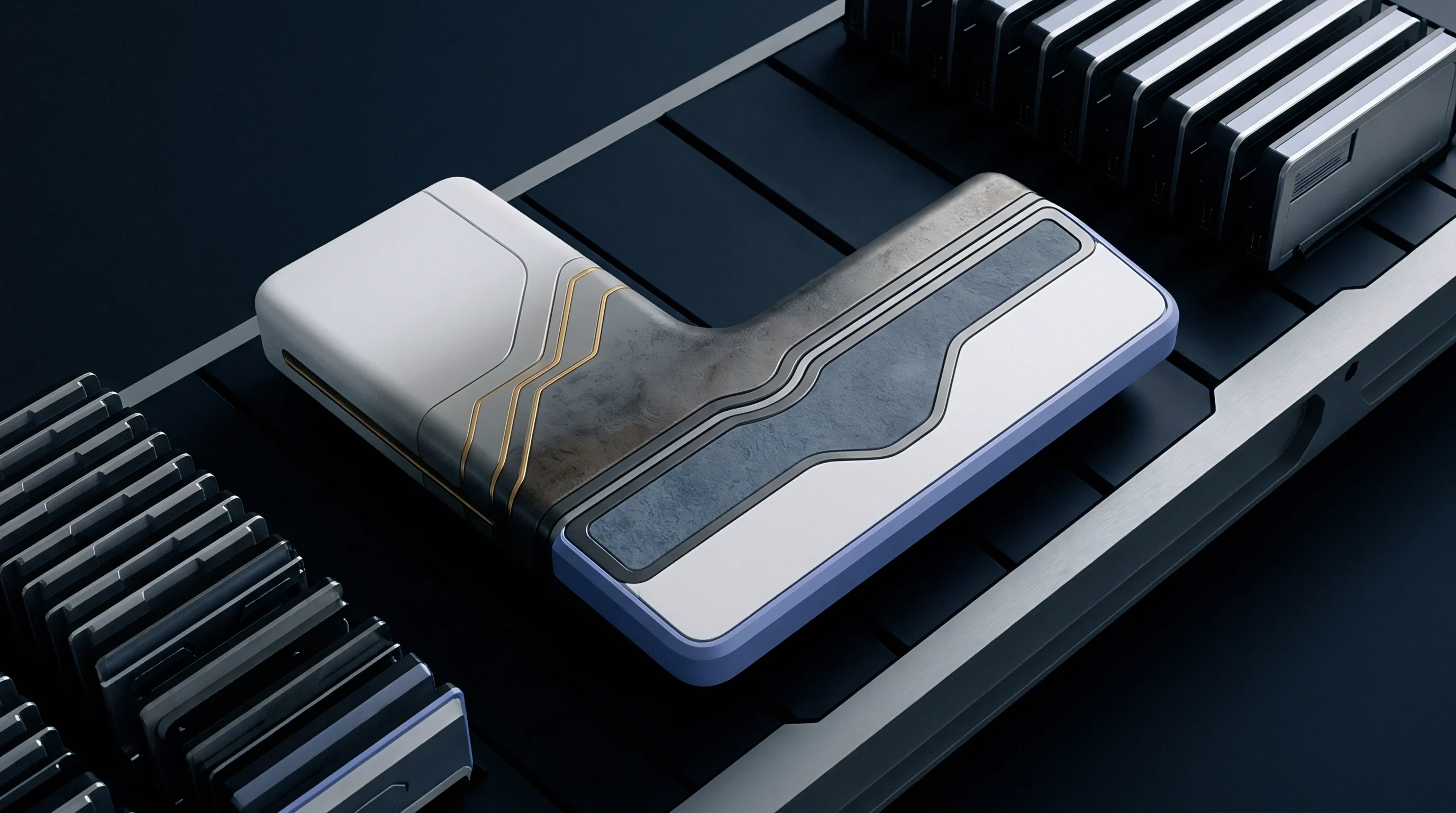
Dislocation Density Scaling within Sub-Micron Current Layers
Lattice defects multiply rapidly inside cold-worked copper contact zones. Conduction electrons traveling through this micro-layer experience intense scattering off dislocation forests and grain boundaries. In undamaged copper at room temperature, the electron mean free path is roughly 39 nm.
When dislocation density rises to 1011 cm-2, the effective electron mean free path drops below 15 nm. Dislocations scatter conduction electrons.
This localized reduction in electron mobility degrades effective electrical conductivity within the skin depth layer by 15 percent to 40 percent compared to bulk theoretical values. StandardRF attenuation models assume uniform bulk conductivity right up to the metal-air boundary, leading to significant underestimation of interface losses at hundred-gigahertz frequencies.
- Yield strain localization creates high dislocation gradients across individual micro-junctions, creating irregular conductivity zones directly in the path of sub-millimeter waves.
- Work hardening saturation occurs at high assembly torques, locking high lattice resistance permanently into the skin depth profile of mated connectors.
- Recrystallization thresholds remain unreached at ambient temperatures, preventing self-healing of damaged conductor crystal structures in industrial RF hardware.
- Grain boundary accumulation forces conduction currents to cross high-energy lattice mismatch boundaries every few nanometers along the surface profile.
Neglecting asperity plastic yield during flange assembly leads to unexpected Insertion Loss spikes that degrade receiver noise performance and compromise system thermal dissipation.


Discontinuity
Spatial variation in lattice strain across mated waveguides creates non-uniform electromagnetic boundary conditions. Because conductivity drops locally at crushed asperity points while remaining near nominal values in surrounding uncontacted troughs, surface impedance varies continuously across nanometer distances.
The surface impedance of a metallic conductor is expressed as Zs = Rs + j Xs, where surface resistance Rs and surface reactance Xs equal sqrtω μ / (2 σ). When local conductivity σ drops due to strain hardening, surface resistance Rs increases. Concurrently, spatial gradients in Rs perturb tangential electric and magnetic field boundary conditions at 100 GHz.

Surface Impedance Expansion and Modified Conductivity Profiles
Electromagnetic excitation at hundred-gigahertz frequencies penetrates only a thin shell of the conducting surface. Surface resistance dominates overall attenuation.
The effective skin depth expands inside deformed work-hardened nodes. Calculating effective skin depth δeff using degraded local conductivity σeff reveals anomalous skin depth expansion from 209 nm up to 270 nm in copper. This expansion forces radio frequency energy deeper into material containing embedded surface oxides, voids, and micro-cracks.
Asperity cold-working increases local surface resistance well beyond standard smooth-wall electromagnetic model predictions.
| Parameter | Pristine Bulk Copper | Elastic Contact Zone | Plastically Deformed Asperity |
|---|---|---|---|
| Dislocation Density (cm-2) | 106 | 107 | 1011 |
| Electron Mean Free Path (nm) | 39.0 | 36.5 | 14.2 |
| Effective Conductivity (S/m) | 5.80 x 10⁷ | 5.45 x 10⁷ | 3.65 x 10⁷ |
| Skin Depth at 100 GHz (nm) | 209 | 215 | 263 |
| Surface Resistance at 100 GHz (Ω/sq) | 0.082 | 0.085 | 0.127 |
Non-Linear Junction Conduction and Harmonic Generation
Native metal oxides create thin tunneling barriers at points where asperities touch. Copper oxide films (Cu2O) measuring 2 nm to 5 nm thick cover un-negotiated surface peaks. Mechanical pressure ruptures these oxides in isolated spots, forming direct metal-to-metal conducting channels called a-spots.
The combination of thin oxide tunneling barriers and localized high current densities across narrow a-spots introduces non-linear current-voltage characteristics. When driven with high transmit power levels (exceeding +15 dBm at 100 GHz), these non-linearities generate passive intermodulation products. Spurious signals appear at intermodulation frequencies, raising the receiver noise floor and degrading channel capacity in multi-carrier sub-terahertz communication systems.
- Tunneling conduction through non-ruptured oxide layers introduces bias-dependent resistance that distorts high-power radio frequency envelopes.
- Current crowding around tiny a-spots elevates local current density, generating localized thermal spikes that further depress local metal conductivity.
- Micro-cavity resonance inside uncontacted surface valleys creates localized reactive energy storage that alters interface phase velocity.
- Oxide breakdown noise generates random low-level phase jitter across high-frequency transceivers.
Component suppliers frequently explain unexpected 100 GHz attenuation by asserting that surface roughness metrics were fully met during manufacturing without acknowledging that mating force induced strain hardening during assembly.
Reach
Propagation performance in high-frequency wireless equipment depends directly on internal RF path losses. In sub-terahertz systems such as IEEE 802.15.3d transceivers or 100 GHz fixed wireless backhaul units, the total available link budget is constrained by semiconductor output power capabilities and thermal limits.
Standard power amplifiers operating at 100 GHz typically yield saturated transmit powers between +10 dBm and +18 dBm. Low-noise receivers achieve noise figures between 6 dB and 10 dB. Unmodeled losses across internal waveguide interconnects and module interfaces directly erode available link margin, reducing clear-weather link distance.

Sub-Terahertz Link Budget Erosion in Industrial Transceivers
Wireless transceivers operating in the hundred-gigahertz spectrum face severe attenuation from atmospheric absorption and passive front-end components. Lattice strain reduces bulk conductivity. RF energy converts to heat.
Consider a 100 GHz point-to-point wireless link operating over a target distance of 100 meters. The transmitter generates +15 dBm output power into a 35 dBi directional horn antenna. The receiver employs a matching 35 dBi antenna with an effective noise bandwidth of 2.16 GHz and a noise figure of 8 dB, yielding an operational sensitivity threshold of -58 dBm for QPSK modulation at a target bit error rate of 10-6.
| Budget Element | Nominal Model Value | Measured Deformed Interface Value | Unit |
|---|---|---|---|
| Transmitter Output Power | +15.0 | +15.0 | dBm |
| TX & RX Antenna Gains (Combined) | +70.0 | +70.0 | dBi |
| Free Space Path Loss (100m, 100 GHz) | -112.4 | -112.4 | dB |
| Atmospheric & Rain Attenuation | -0.5 | -0.5 | dB |
| Internal Flange Interfaces (4 Mated Pairs) | -0.8 | -6.8 | dB |
| Net Power at Receiver Input | -28.7 | -34.7 | dBm |
| Receiver Sensitivity (16-QAM, 10 Gbps) | -48.0 | -48.0 | dBm |
| Operating Link Margin | +19.3 | +13.3 | dB |

How Does Micro-Yielding Alter Millimeter Wave Insertion Loss?
Waveguide attenuation models calculated from bulk metal conductivity assume smooth conductor walls. Standard calculations assign a nominal attenuation of roughly 0.2 dB per flange pair at 100 GHz (WR-10 guide size). However, when mounting hardware is torqued down, plastic deformation across contacting asperities creates a high-resistance surface layer.
Phase shifts distort high-order modulation.
Four mated flange interfaces reside in a typical transceiver signal path: power amplifier to filter, filter to diplexer, diplexer to feedhorn, and external antenna flange. Under nominal assumptions, these four interfaces contribute 0.8 dB total insertion loss. Calculated attenuation underestimates real loss.
When plastic deformation expands skin depth and increases surface resistance from 0.082 Ω/sq to 0.127 Ω/sq across crushed asperities, the actual loss per flange pair increases to 1.7 dB. Total interface loss surges to 6.8 dB. Impedance shifts destroy link margin.
The unexpected 6.0 dB interface penalty reduces link margin significantly. To compensate, transceivers must drop high-order QAM modulations in favor of lower-order modulations like QPSK, effectively halving system data throughput from 20 Gbps to 10 Gbps.
Unmodeled flange interface loss can force high-capacity sub-terahertz transceivers to fall back to lower modulation schemes, cutting link data rates in half.
The extent to which cyclic thermal expansion in outdoor environments progressively alters asperity contact area and worsens non-linear passive intermodulation over years of service remains an active field of study.

Verification
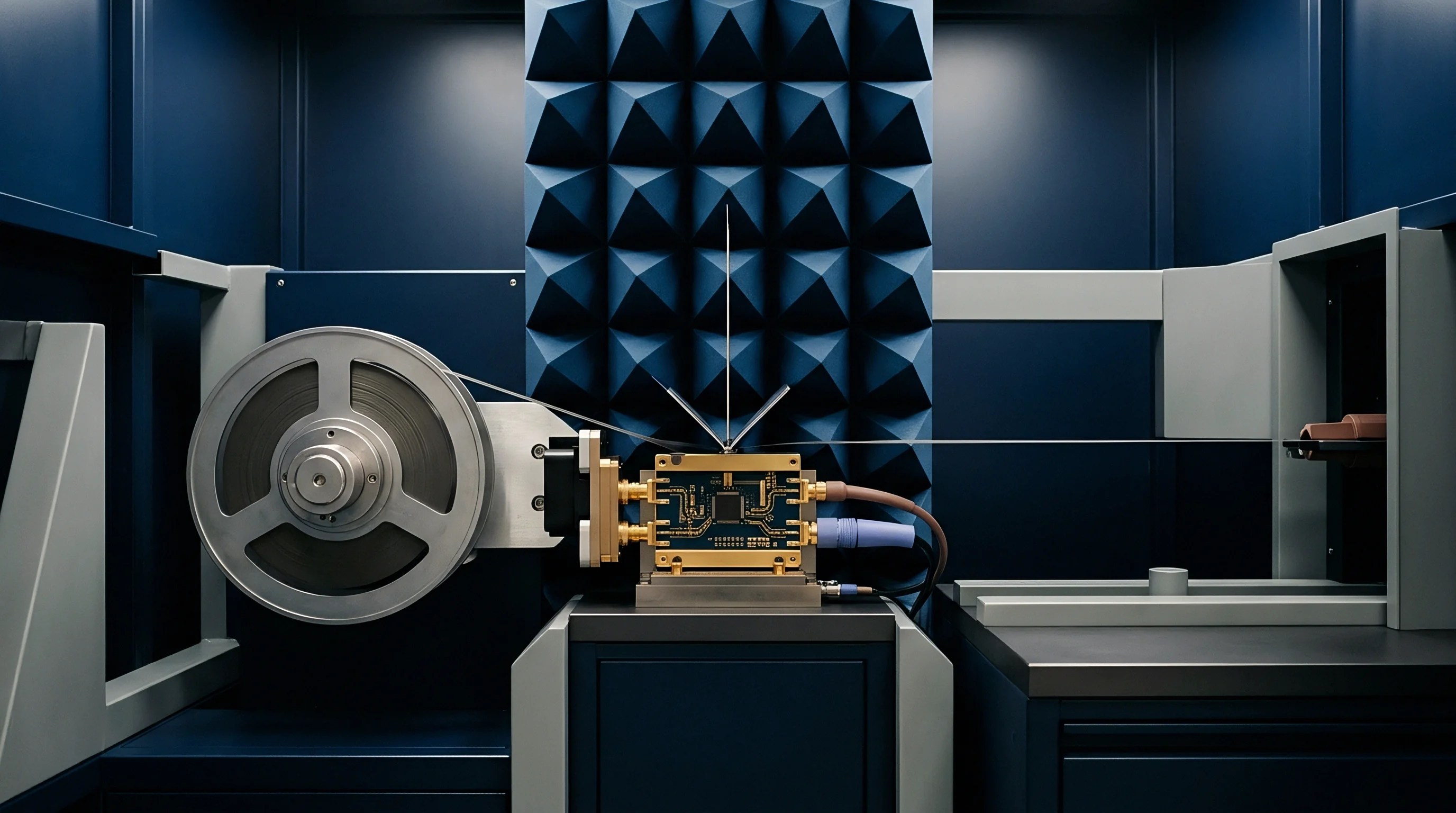
High-frequency bench characterization demands specialized equipment capable of isolating sub-millimeter wave attenuation mechanisms. Bench testing exposes unmodeled dissipation.
Measuring the electromagnetic effect of plastically deformed asperities requires distinguishing between bulk dielectric losses, alignment errors, and surface conduction degradation. Standard two-port vector network analyzer measurements must be augmented with high-resolution surface profilometry and localized micro-probing.

Vector Network Analyzer De-Embedding for Flange Interfaces
Scattering parameter measurements above one hundred gigahertz require advanced calibration routines to eliminate probe and cabling effects. Vector network analyzers utilize frequency multipliers to cover the 75 GHz to 110 GHz band (W-band) and 110 GHz to 170 GHz band (D-band).
Calibration relies on Thru-Reflect-Line (TRL) or Multiline TRL standards executed on ultra-precise sapphire or alumina calibration substrates. To isolate flange interface loss from waveguide line attenuation, test setups employ variable-length precision waveguides. By comparing S-parameters across multiple waveguide lengths under tightly controlled bolt torques, engineers isolate the precise insertion loss contributed by the interface skin depth anomalies.

Atomic Force Profilometry and Surface Conductivity Mapping
Topographical mapping instruments evaluate surface roughness down to nanometer dimensions. Atomic Force Microscopy (AFM) measures surface parameters including root-mean-square roughness (Rq), average roughness (Ra), and mean surface slope (SΔ q). Sub-terahertz links demand extreme precision.
Coupling topographical AFM data with Conductive Atomic Force Microscopy (C-AFM) allows simultaneous measurement of local contact resistance across individual asperities before and after mechanical loading. Testing demonstrates that regions subjected to compressive stresses above the yield strength exhibit reduced localized conductivity corresponding directly to strain-hardened crystal regions.
- Mount the polished waveguide test sample into an optical white light interferometer to record baseline surface roughness profiles prior to physical contact.
- Secure the waveguide flange into a micro-positioning test fixture equipped with calibrated load cells to monitor applied clamping force continuously.
- Apply specified mounting torque sequentially using a calibrated digital torque screwdriver while tracking real-time compressive load across the flange face.
- Execute a multi-line TRL calibration on the vector network analyzer across the full 100 GHz to 140 GHz sweep range.
- Measure two-port S-parameters, extracting S21 insertion loss and S11 return loss across multiple mating cycles to quantify strain hardening hysteresis.
- Unclamp the flange assembly and re-examine the contact face under atomic force microscopy to map plastic deformation zones and permanent micro-yield indentations.
Surface roughness values measured before assembly provide zero guarantee of RF performance if mounting torque exceeds material yield limits during installation.

Sourcing
Procurement documents for high-frequency radio components need explicit mechanical and metallurgical criteria. Standard drawing notes specifying basic dimensions and generic gold plating are insufficient for 100 GHz hardware.
Sourcing engineers must balance surface smoothness against material hardness. Gold plating prevents rapid oxidation. However, excessively soft gold layers yield easily under low bolt torques, creating large plastic deformation zones that lower conductivity.
Over-tightening permanently crushes micro-structures. Tighter tolerances elevate production costs.
Plating Metal Specs and Interface Torque Controls
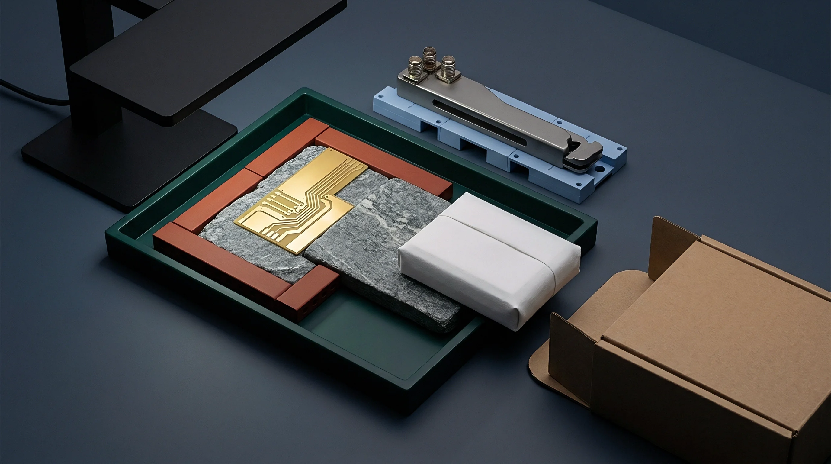
Surface plating selection determines both micro-hardness and oxidation susceptibility for high-frequency mating faces. Standard Electroless Nickel Immersion Gold (ENIG) provides excellent corrosion resistance, but the underlying nickel layer introduces severe magnetic and ohmic losses at 100 GHz due to nickel’s low conductivity and high permeability.
Direct Hard Gold plating applied over non-magnetic copper substrates represents a superior choice. Hard gold alloys incorporating trace cobalt or nickel (0.1 percent concentration) increase surface hardness from 60 HV (Vickers Hardness) up to 150-200 HV. This elevated hardness increases micro-yield strength, preventing plastic deformation of asperities under standard mating pressures.
Immersion Silver plating provides high conductivity (σ = 6.3 × 10⁷ S/m) and low hardness, but demands anti-tarnish packaging and strict operational controls to prevent atmospheric sulfur contamination during assembly.
Acceptance Metrics for Sub-Millimeter Interconnect Lots
Quality management programs for hundred-gigahertz hardware incorporate both mechanical surface metrics and RF insertion loss screening. Component specifications must define maximum allowable clamping torque, surface roughness limits, and plating micro-hardness ranges.
Purchase orders for 100 GHz waveguide assemblies should explicitly mandate Direct Hard Gold plating over copper with a Vickers hardness exceeding 140 HV and specify maximum assembly torque limits to prevent skin depth degradation.
A representative procurement contract clause covering high-frequency interface quality specifies:
All mating flange surfaces operating above 90 GHz shall feature Direct Hard Gold plating over copper with a minimum thickness of 1.27 micrometers and a deposit hardness between 140 HV and 200 HV per ASTM B488 Type II. Flange surface roughness shall not exceed Rq = 80 nanometers as measured by optical white light interferometry over a 100 x 100 micrometer evaluation area. Assembly drawings shall specify a maximum fastener mounting torque of 0.15 Newton-meters; exceeding this limit voids component insertion loss warranties and invalidates factory calibration data.