Evaluating Antenna Impedance Matching and Board Layout Strategies for Embedded Transceivers
Evaluating embedded transceiver matching and layout requires conjugate source matching, coplanar ground stitching, and in-housing impedance tuning.

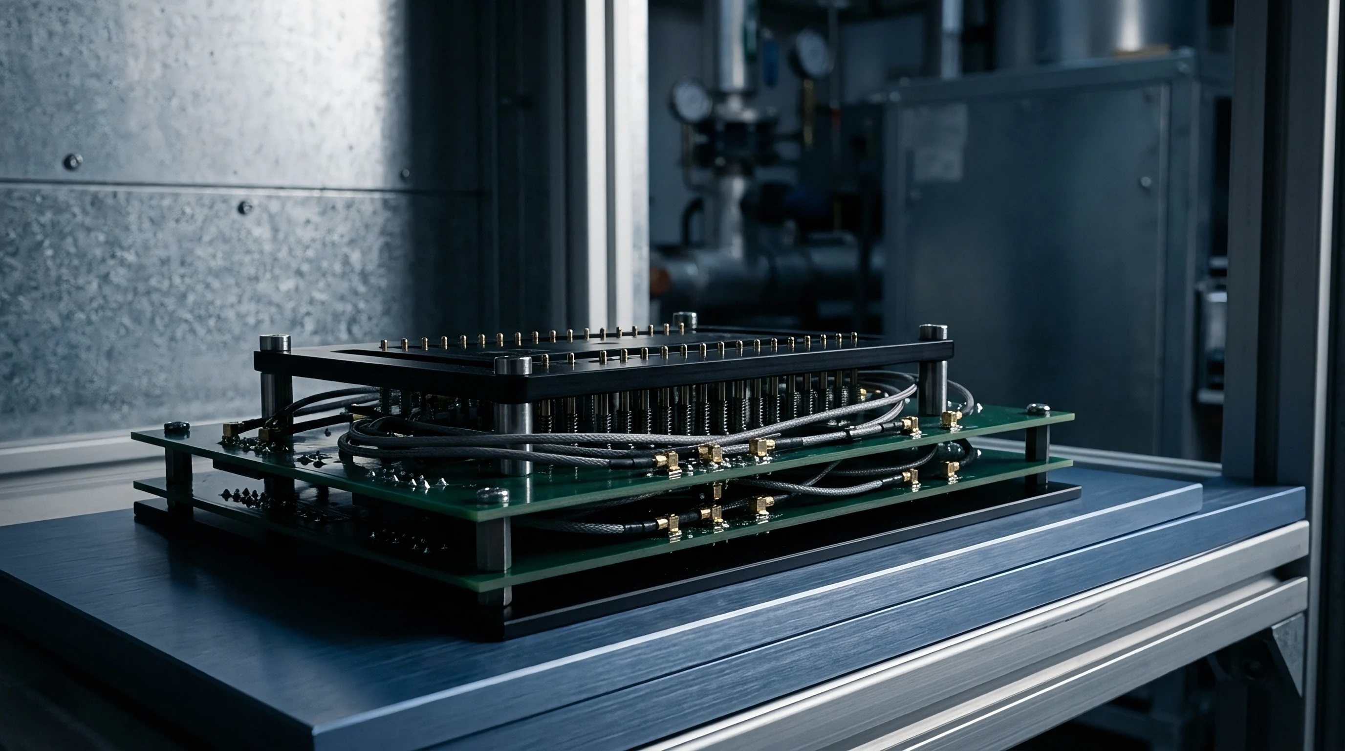
Topology
Integrated transceiver front ends present source impedances that rarely equal pure fifty-ohm resistive loads across operating frequencies. Silicon vendors specify optimum load pull impedances, often complex numbers such as twenty-two plus j twenty-four ohms, to extract maximum output power while maintaining power-added efficiency. Conjugate matching dictates presenting the complex conjugate of this transceiver source impedance to the network, transforming the complex conjugate load back to the nominal characteristic impedance of the transmission line feeding the radiator.
RF matching structures rely on three fundamental passive component arrangements: the two-element L-network, the three-element Pi-network, and the three-element T-network. Selecting among these options governs bandwidth, harmonic attenuation, and bill-of-materials sensitivity.
- Two-element L-networks provide the lowest insertion loss and simplest topology for narrow bandwidth applications. One series reactive element pairs with one shunt reactive element, fixing the circuit quality factor strictly as a function of the impedance transformation ratio.
- Three-element Pi-networks introduce an independent degree of freedom for circuit selectivity. Two parallel shunt capacitors sandwiching a series inductor form a low-pass structure that suppresses second and third transceiver harmonics effectively.
- Three-element T-networks favor high-pass filtering or situations requiring high series reactance. Two series reactive components surround a central shunt leg, reducing sensitivity to stray pad capacitance when transforming very low real impedances upward.
- Discrete balun transformers convert balanced differential transceiver pins to single-ended unbalanced transmission lines. Ceramic multilayer baluns save board area, whereas discrete LC lattice structures permit fine-grained balancing of phase and amplitude errors at half the component procurement expense.
Discrete LC networks introduce insertion loss through finite component quality factors. Inductor equivalent series resistance dominates this attenuation, turning transmitter power into board heat before radiated emission occurs.
A three-element Pi-network designed for 2.45 GHz with low-Q ceramic inductors drops radiated power by 1.4 dB before the antenna feedline.
Bandwidth boundaries restrict narrow networks when transceivers jump channels across broad allocations. Sub-GHz operations spanning 863 MHz to 928 MHz demand wideband impedance transformation. Single-stage L-networks deliver loaded quality factors exceeding ten when transforming twenty ohms to fifty ohms, constraining the usable bandwidth below sixty megahertz.
Dual-stage transformation topologies lower the loaded quality factor of each individual stage, widening overall network response at the expense of two additional passive components.
Differential transceiver architectures eliminate the common-mode ground noise generated by power amplifier switching currents. Interfacing differential transceiver ports directly to balanced dipoles removes the balun completely, saving board surface and bill-of-materials lines. Unbalanced antennas such as quarter-wave monopoles, inverted-F antennas, and ceramic patches mandate conversion back to single-ended geometry, forcing the designer to choose between ceramic integrated baluns and discrete passives.
Engineers calculate discrete LC baluns as lattice networks using two capacitors and two inductors to impart positive and negative ninety-degree phase shifts across adjacent legs. Component tolerance dispersion within these lattice networks creates phase imbalance exceeding eight degrees when standard five-percent passives populate the board. Phase error degrades transceiver receiver sensitivity by degrading common-mode rejection against co-located digital switching harmonics.
Transceiver vendors publish recommended matching values inside reference application notes. These component values assume a rigid board stack-up, precise copper thickness, and specific passive part numbers. Deviations in dielectric height alter stray pad capacitance, invalidating reference values before first prototype bring-up.
The designer uses the reference schematic values strictly as an initial analytical boundary condition.
RF matching networks demand methodical evaluation across transmitter output power, harmonic suppression, receiver noise figure, and board real estate. Compromising harmonic suppression to gain radiated fundamental power risks regulatory rejection during formal telecommunications conformance testing.
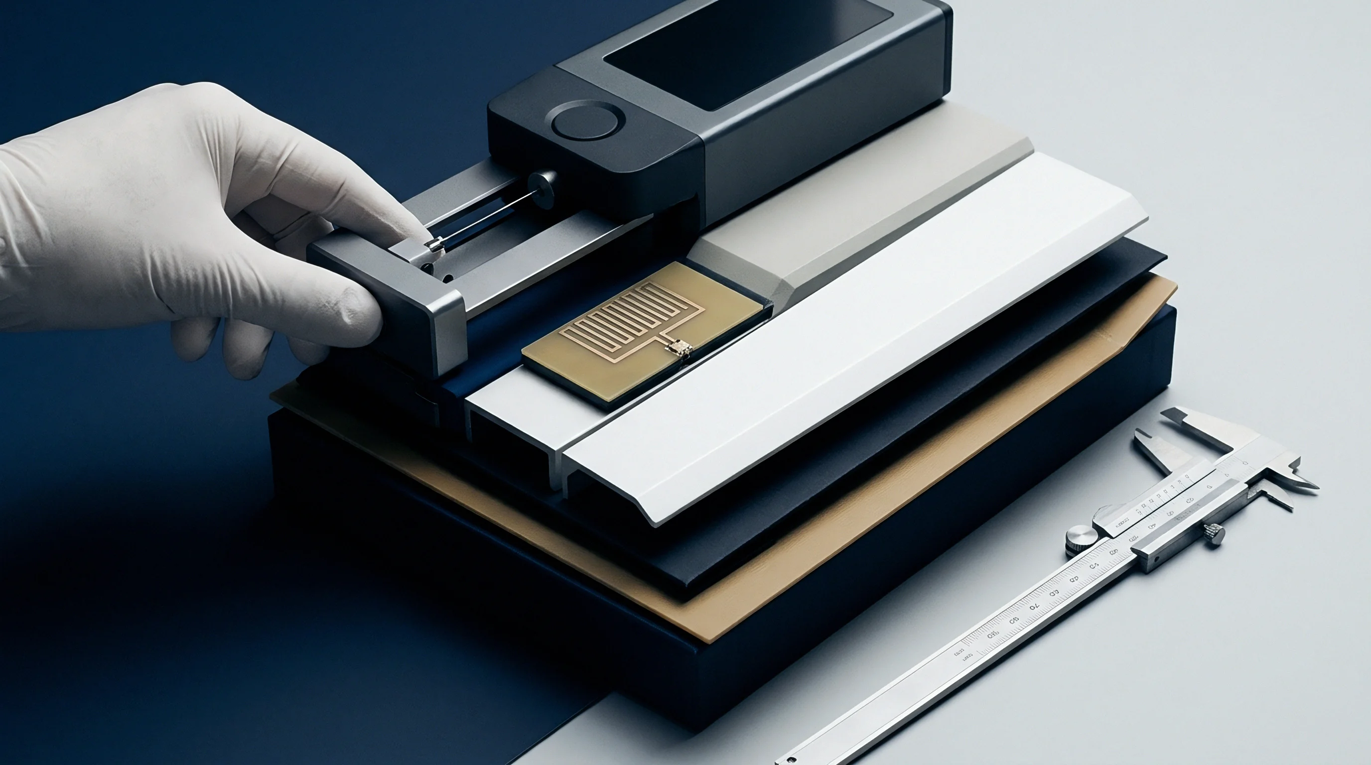
Copper
Physical trace geometry over reference planes establishes electromagnetic wave propagation boundaries. Microstrip lines locate conductors on the outer layer separated from a solid reference plane beneath by dielectric core or prepreg. Grounded coplanar waveguides route the RF conductor between lateral ground pours on the same outer layer, backed by a sub-surface ground return plane.
Lateral ground fences compress field lines within the planar dielectric, reducing stray coupling into adjacent digital signal paths.
Signal traces traversing board layers demand unbroken return paths directly underneath. Gaps or splits in the reference plane force return currents to detour around physical voids, expanding current loop areas exponentially. Expanded loop areas generate parasitic series inductance, radiating magnetic fields that fail spurious emission limits and collapsing transmission line characteristic impedance from fifty ohms to over eighty ohms locally.
A break in the reference plane beneath a 50-ohm RF trace increases return loop inductance and degrades return loss by more than 12 dB.
Ground stitching vias control return current impedance across multi-layer circuit boards. Radio frequency currents follow paths of minimum inductance rather than minimum resistance, clinging directly beneath the signal conductor. Positioning stitching vias alongside coplanar ground planes maintains plane-to-plane ground parity.
Spacing stitching vias at intervals less than one-tenth of the guided wavelength prevents resonant cavity modes from forming between substrate layers.
Coplanar ground spacing requires careful mathematical derivation. Setting lateral copper spacing equal to the trace width creates tight field confinement, but etching tolerances in standard printed circuit manufacturing produce variations in line spacing up to twenty percent. Loose coplanar spacing, set to three times the dielectric height above the reference plane, stabilizes characteristic impedance against lateral etching errors while retaining plane-to-plane isolation.
| Transmission Line Structure | Trace Width (mm) | Ground Spacing (mm) | Loss at 2.4 GHz (dB/inch) | Manufacturing Sensitivity |
|---|---|---|---|---|
| Standard Microstrip (Layer 1 to 2) | 0.34 | None | 0.28 | Low |
| Grounded Coplanar Waveguide | 0.26 | 0.20 | 0.34 | High |
| Buried Stripline (Layer 2 to 3) | 0.18 | None | 0.42 | Moderate |
| Loosely Coupled Coplanar | 0.31 | 0.50 | 0.29 | Low |
Layer stack-up definition determines board impedance reproducibility across manufacturing lots. Four-layer designs placing ground on Layer 2 provide thin dielectric separation to outer RF traces, yielding narrow fifty-ohm lines suitable for direct soldering to compact surface-mount passives. Six-layer and eight-layer boards permit dedicated internal ground and power planes, isolating baseband digital switching buses from sensitive transceiver low-noise amplifier inputs.
Passive matching component mounting pads introduce parasitic shunt capacitance to ground planes beneath. A standard 0402 surface-mount capacitor pad creates roughly 0.08 picofarads of stray capacitance to an adjacent ground plane located 0.15 millimeters below. Removing copper reference planes directly beneath matching component pads, an engineering technique termed ground cutout or anti-pad etching, neutralizes this stray shunt capacitance.
Anti-pad cutouts allow the designer to use matching component values derived from Smith chart calculations without unmodeled parasitic low-pass attenuation.
Thermal relief spokes on RF ground pads generate parasitic series inductance. Ground pins of shunt matching capacitors and transceiver center ground paddles require direct, unbroken copper connections into solid copper pours. Multiple vias drop current directly from the center thermal ground paddle of the transceiver integrated circuit to the internal plane, minimizing common-mode ground bounce during high-power transmission bursts.
Routing RF lines adjacent to switched-mode power supply inductors induces magnetic phase noise into transceiver frequency synthesizers. Maintaining a minimum physical separation of five millimeters between switched-mode power inductors and the RF trace line suppresses magnetic induction coupling below ninety decibels.
Board fabricators modify outer copper weights during plating processes, introducing trace thickness variations. Standard one-ounce copper begins as half-ounce base foil that gains electroplated copper during barrel plating. Plating baths deposit uneven copper thicknesses across panel perimeters compared to panel centers, skewing characteristic impedance by up to three ohms across production panels.
Etch compensation factors must sit within the production files sent to the manufacturing floor.


Parasitics
Non-ideal electrical behaviors inside passive components compromise matching networks as operational frequencies scale into gigahertz territory. Surface-mount resistors, inductors, and capacitors contain internal equivalent series resistance, equivalent series inductance, and shunt capacitance dictated by packaging geometry and dielectric chemistry.
Inductors experience self-resonance where internal winding capacitance balances designed series inductance. Above this self-resonant frequency, the component behaves as a capacitor, inverting phase shift and destroying matching network synthesis. Multilayer ceramic inductors demonstrate lower self-resonant frequencies and lower quality factors than wire-wound ceramic alternatives, yet wire-wound parts introduce higher unit procurement costs and directional assembly sensitivities.

Do Inductor Resonances Degrade High Harmonic Suppression?
Operating matching networks near component resonance modes causes harmonic filtering to fail. Wire-wound inductors chosen for fifty-ohm matching at 915 MHz often exhibit self-resonance near 2.7 GHz, precisely where third-harmonic energy resides. Near resonance, component impedance spikes and then drops, allowing third-harmonic emissions to bypass attenuation filters and breach radio emissions regulations.
Capacitor dielectric material directly governs equivalent series resistance and temperature drift. Class 1 dielectric ceramics such as C0G and NP0 maintain capacitance stability within thirty parts per million per degree Celsius across standard operational temperature ranges. Class 2 dielectrics like X7R provide higher volumetric capacitance density, but their dielectric constants shift dramatically under applied direct-current voltage bias and thermal cycling, detuning matching networks in outdoor field deployments.
| Component Technology | Case Size | Quality Factor (Q) at 2.4 GHz | Self-Resonant Frequency (GHz) | Tolerance Band |
|---|---|---|---|---|
| Wire-Wound Ceramic Inductor | 0402 | 55 to 80 | 6.0 | ±2% |
| Multilayer Ceramic Inductor | 0402 | 18 to 28 | 3.8 | ±5% |
| Thin-Film Ceramic Inductor | 0201 | 22 to 32 | 4.5 | ±1% |
| C0G/NP0 Ceramic Capacitor | 0402 | 250 to 400 | 7.2 | ±0.1 pF |
| X7R Ceramic Capacitor | 0402 | 20 to 45 | 2.1 | ±10% |
Printed circuit board base materials introduce significant dielectric variability. Standard FR-4 epoxy-fiberglass substrates present dielectric constants ranging from 4.0 to 4.6 depending on glass weave tightness and resin content. At 2.4 GHz, signal traces traversing areas of dense glass yarn encounter higher relative permittivity than traces running over pure resin pockets, skewing phase velocity and trace characteristic impedance across identical boards within one fabrication panel.
Glass weave skew affects high-frequency phase alignment in differential RF lines. Spread-glass fabrics such as 1078 or 1067 mitigate this weave effect by distributing fiberglass yarn uniformly across the prepreg sheet. High-frequency hydrocarbon ceramic laminates eliminate the glass weave problem altogether and reduce dielectric dissipation factors by an order of magnitude, though base laminate panel costs increase fourfold relative to FR-4.
IPC-4101 specification sheets permit dielectric constant tolerances of plus or minus ten percent on standard FR-4 laminates, which shifts transmission line impedance by two ohms.
Solder mask coatings apply an uncharacterized dielectric over the outer copper traces. Liquid photoimageable solder masks exhibit relative dielectric constants between 3.3 and 3.8 with loss tangents near 0.02 at microwave frequencies. Applying solder mask over a coplanar waveguide lowers trace characteristic impedance by two to three ohms and increases transmission loss by 0.1 dB per centimeter at 5.8 GHz.
High-precision designs apply solder mask clearance windows over RF traces and matching components to preserve bare copper propagation conditions.
Parasitic pad capacitance alters Smith chart rotation. When evaluating matching topologies, engineers must treat the physical solder pad as an open-ended transmission line stub or a lumped shunt capacitance to ground. Omitting pad parasitics from circuit simulations forces empirical component swapping on the lab bench during hardware qualification.
The relationship between component tolerances and production yield dictates strict bill-of-materials boundaries. Monte Carlo simulations across two-percent tolerance components demonstrate minimal insertion loss dispersion. Substituting five-percent tolerance parts expands the impedance locus distribution circle, causing fifteen percent of finished boards to exceed acceptable voltage standing wave ratio limits.
Tolerances stack across capacitors, inductors, board etching, and laminate permittivity. Sourcing departments trading high-grade C0G capacitors for lower-tier second sources introduce systematic impedance offsets that factory line testing flags as transceiver receiver sensitivity degradation. Engineering approval criteria must govern component substitutions across all passive matching lines.


Detuning
Antenna elements operate as open electromagnetic resonators whose reactive fields interact with neighboring materials. Bringing an embedded antenna into physical proximity with product enclosures, batteries, displays, or human tissue loads the near field, altering the feed point impedance and pulling the center resonant frequency away from the intended operating band.
Dielectric loading slows electromagnetic wave propagation along the radiating element. Plastic housings made from polycarbonate, ABS, or nylon introduce relative dielectric constants ranging from 2.5 to 3.5 within the reactive near field. This dielectric medium electrically lengthens the radiating structure, systematically shifting resonant frequencies downward.

Will Housing Plastics Shift Resonant Frequency Downward?
Encasing an antenna in an injection-molded enclosure shifts the center resonance downward by three to eight percent depending on wall thickness and clearance. An inverted-F antenna tuned for 2.45 GHz in free air shifts to 2.32 GHz inside a tightly fitted polycarbonate casing, destroying return loss at the desired operating band unless pre-compensated during board layout.
Battery packs, metallic shields, and large electrolytic capacitors present conductive ground boundaries that alter radiation resistance. Placing an antenna element within five millimeters of a lithium-ion battery cell shorts out electric fields, collapsing radiation efficiency below thirty percent. Conductive elements within the near-field volume act as parasitic reflectors, reshaping omnidirectional antenna radiation patterns into irregular lobes with deep coverage nulls.
Matching networks must compensate for enclosure-induced impedance shifts. When designing custom embedded antennas, engineers measure complex antenna feed point impedance inside the fully assembled final enclosure using vector network analyzers. The matching network is then synthesized to transform this loaded, detuned impedance back to fifty ohms, rather than matching an antenna standing in free air.
- Calibrate network analyzer reference planes using a coaxial calibration kit up to the board-edge interface. Solder a semi-rigid pigtail coaxial cable to the antenna feed point, cutting the transceiver trace connection cleanly.
- Embed the calibrated board inside the production housing, securing all mechanical fasteners, battery clips, and display cables. Keep fingers clear of radiating elements during initial reflection coefficient captures.
- Measure reflection coefficients across the target frequency band, exporting two-port touchstone files containing real and imaginary impedance values. Record minimum return loss frequencies and bandwidth boundaries.
- Synthesize the matching network on a Smith chart, introducing series and shunt reactive elements that pull the loaded antenna impedance point to the chart center. Verify that the required component values exist in standard commercial component series.
- Populate the calculated passive component values onto the board matching pads. Reassemble the complete enclosure and re-measure return loss to confirm that the voltage standing wave ratio remains below 2.0 to 1 across the operational channel allocation.
Human interaction introduces dynamic, unpredictable detuning. Hand placement over a wearable device or handheld terminal introduces both dielectric loading and high conductive absorption losses. Human tissue exhibits relative permittivity near 38 and conductivity near 1.5 siemens per meter at 2.4 GHz, absorbing radiated energy into thermal dissipation.
Wideband antenna structures tolerate human body detuning better than high-Q narrow-band matching structures, as their operating bandwidth accommodates frequency shifts without dropping connection links.
Vector network analyzer measurements require meticulous calibration techniques. Semi-rigid coaxial pigtails soldered to board test points disrupt local ground planes if ground braids are poorly bonded. Ferrite beads clamped along the exterior of test coaxial cables choke off antenna currents travelling back down the outer shield, eliminating test cable radiation artifacts from return loss plots.
Over-the-air testing inside anechoic chambers validates true radiated performance after matching completion. Total Radiated Power measures transmitter output efficiency across three-dimensional spatial coordinates, accounting for both matching loss and antenna efficiency. Total Isotropic Sensitivity evaluates receiver performance in the presence of internal system noise, revealing baseband processor harmonic interference that conducted bench measurements cannot detect.
Enclosure material variations between prototype rapid-tooling resin prints and production injection-molded plastics generate testing discrepancies. Stereolithography resins present different dielectric loss tangents than production polycarbonates, meaning matching networks optimized on early mechanical prototypes will drift out of alignment when production tooling ships.
Component tolerance drift within matching passives compounds mechanical enclosure assembly variations. Enclosure wall thickness tolerances of ten percent translate to three-picofarad shifts in effective near-field loading. Sourcing contracts must lock enclosure resin formulations, pigment masterbatches, and wall thickness tolerances to safeguard wireless link margins.

Release
Moving an embedded transceiver design from engineering bench prototyping to full-volume production transfer requires an exhaustive, unambiguous technical transfer dossier. Miscommunication regarding board stack-ups, component ratings, or test procedures introduces catastrophic line yield losses and schedule delays during factory bring-up.
The manufacturing package contains exact copper geometry, drill tables, solder mask layers, and stack-up specifications. Delivering Gerber X2 or IPC-2581 files conveys layer stack-up definitions, material properties, and impedance-controlled trace callouts directly inside machine-readable metadata. Traditional RS-274X Gerber files strip netlist and layer sequencing intelligence, leaving stack-up dielectric heights open to factory interpretation.
Stack-up documentation defines core and prepreg thicknesses, copper weights, and target trace characteristic impedances with explicit tolerance windows. Printed circuit board fabricators must tune trace widths to match dielectric resin content variations across production runs. Contract terms must dictate that the fabricator run impedance coupon verification on every panel, archiving test coupons for sixty days post-shipment.
Production test coupons mirror the exact RF trace geometry, matching pad layout, and ground return transitions used inside the transceiver section. Testing coupons along panel breakaway rails enables automated time-domain reflectometry screening without requiring probe access to miniaturized, crowded production boards. Panels exhibiting coupon characteristic impedance outside a plus or minus five percent window face immediate line rejection.
Factory bill-of-materials documentation demands strict component manufacturer part number callouts. Sourcing teams cannot authorize generic passive component substitution on RF matching lines. Passive substitutions with identical nominal capacitance values but inferior high-frequency quality factors or shifted self-resonant points degrade transceiver output power and sensitivity across production lots.
Production line test architectures balance test coverage against station cycle time. Conducted testing through automated RF switch matrices provides precise measurements of transmitter power, frequency error, phase noise, and receiver sensitivity. Radiated testing inside compact benchtop shielded boxes verifies total assembly integration, confirming that internal antenna connections, enclosure assembly, and matching networks function harmoniously.
A contract line specifying IPC-6012 Class 3 impedance tolerances binds the PCB fabricator to five-percent impedance limits across all production panels.
Non-recurring engineering line items on assembly quotes must delineate exact testing deliverables. Sourcing agreements must explicitly divide responsibilities between design owners and manufacturing facilities regarding test fixture development, golden unit calibration schedules, and firmware flashing protocols during functional testing.
Second-source board fabricator qualifications require full re-characterization of RF front-end performance. Identical Gerber data transferred to a secondary fabrication facility will encounter different prepreg resin formulations, base copper foil roughness, and etch bath chemistries. Engineering change control workflows must mandate vector network analyzer impedance verification and conducted power tests on twenty sample boards from any new manufacturing source prior to commercial volume authorization.
Regulatory compliance certificates bind physical hardware layouts directly to authorized filings. Changing a matching passive value, altering a trace route, or substituting an antenna radiator invalidates existing telecommunications equipment authorizations under FCC Part 15 or European RED directives. Class II permissive changes demand re-testing spurious radiated emissions at accredited test laboratories, incurring additional non-recurring expenses and eight-week regulatory review queues.
The transfer dossier forms the binding contractual baseline between buyer and contract manufacturer. Ambiguities left inside layer stack-up drawings or passive component substitution allowances convert directly into scrap costs when manufactured lots fail final wireless screening tests. Precision in the technical release preserves link margins, factory yields, and product launch timelines.