Meaning
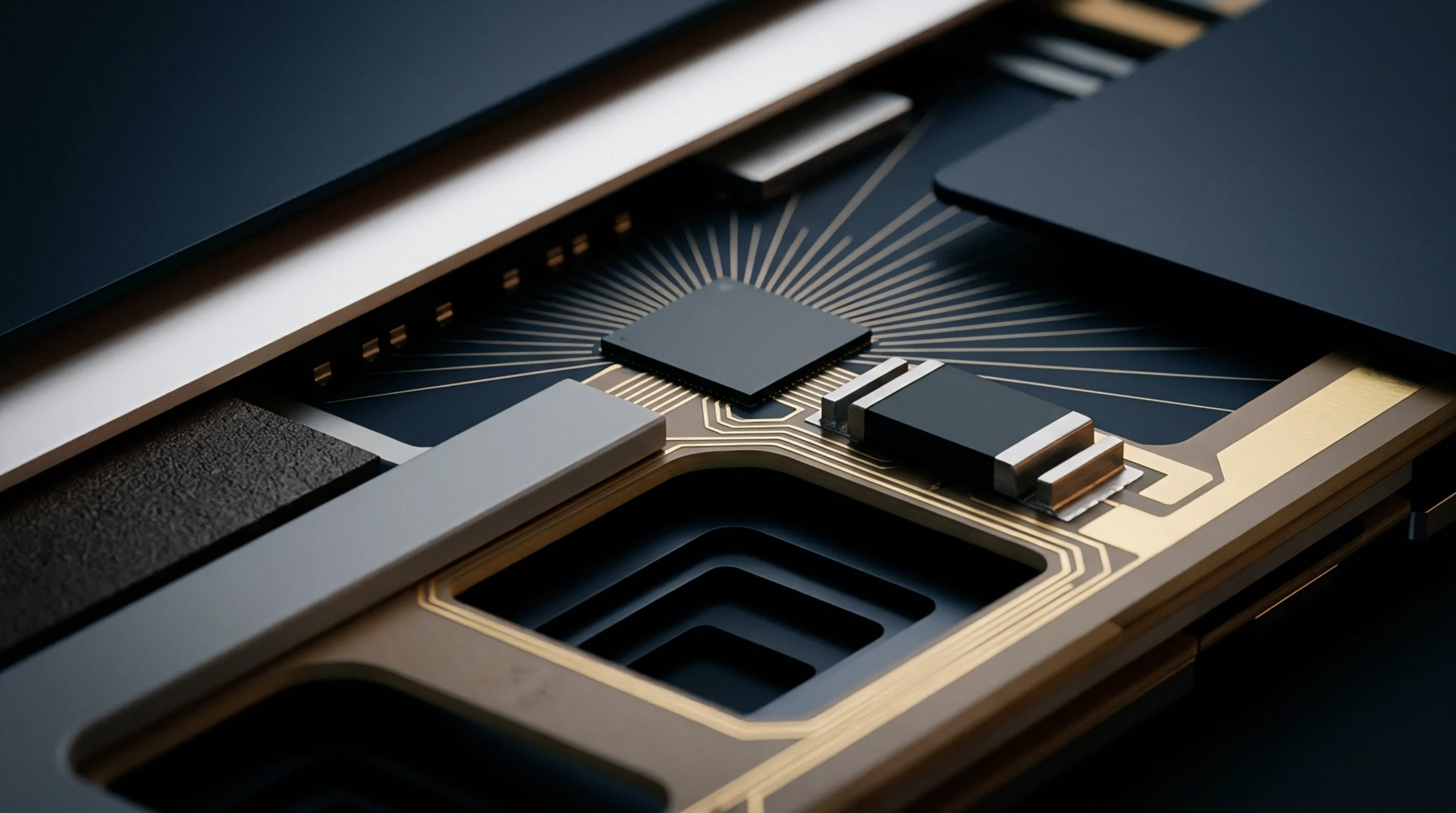
Computer aided manufacturing file format extends the standard printed circuit board description by adding metadata that identifies layer functions, drill hole attributes, and component positions. This enhancement over the older RS-274X standard eliminates the need for separate, often confusing, text files to explain the purpose of each layer. By using gerber x2, the designer can explicitly state whether a layer is a top copper, a solder mask or a legend, which reduces the risk of errors during the fabrication process.
The format is fully backward compatible, meaning that older machines can still read the vector data while newer systems can take advantage of the added intelligence. This standardization is a major step toward full automation in the production of electronic assemblies. It ensures that the manufacturer has all the information needed to build the board without constant communication with the designer.
Data Attribution
Inclusion of specific properties for every geometric shape in the file allows the manufacturing software to understand the design intent. In the gerber x2 format, a pad can be identified as a surface mount land, a through hole or a fiducial mark. This attribution is valuable because it allows the fabrication house to automatically apply the correct tolerances and finishes to each feature.
For example, the software can identify via holes and ensure they are properly plugged or tented as required. Without this metadata, the technician would have to manually identify these features, which is time consuming and prone to error. The added clarity ensures that the finished board matches the original vision of the engineer.
Stackup Definition
Arrangement of the copper and dielectric layers is clearly defined within the file structure to prevent assembly mistakes. The gerber x2 format includes a specific command that describes the order of the layers, their thickness and the material properties. This information is historically sent in a separate spreadsheet or a drawing, which can easily be mismatched with the actual data files.
By embedding the stackup inside the gerber data, the risk of building the board upside down or with the wrong impedance is greatly reduced. The manufacturing system can automatically verify that the files are complete and in the correct order before the first piece of copper is etched. This self-validating nature of the format is a significant benefit for high speed designs where layer order is critical.
Fabrication Instruction
Streamlining the communication between the design desk and the factory floor reduces the lead time for new prototypes. Because gerber x2 provides a single, unambiguous source of truth, the manufacturer can generate a quote and start production much faster. The format also includes information about the panelization and the locations of the components, which helps with the automated assembly process.
If a problem is detected in the file, the software can pinpoint the exact location and attribute, making it easier for the designer to fix the issue. This efficiency is particularly important in the fast paced world of consumer electronics where a delay of a few days can be costly. Adopting this standard is a sign of a mature and professional design workflow.
It provides the foundation for higher quality, more reliable hardware.