Quantifying Semicustom Wireless Module Non Recurring Engineering Cost Break Even Thresholds
Semicustom module break-even hinges on balancing upfront engineering charges against unit bill-of-material reductions across projected volume thresholds.


Arithmetic
Determining whether a semicustom module makes financial sense comes down to balancing upfront non-recurring engineering fees against per-unit bill-of-materials deltas. Standard wireless modules avoid initial design charges entirely, but their unit prices carry supplier overhead and licensing margins. Moving to a semicustom design concentrates costs into upfront engineering while lowering per-unit production expense by stripping unneeded circuitry, selecting leaner parts, and tightening the board layout.
Semicustom projects accumulate engineering hours rapidly across board re-layouts, RF matching simulations, tooling for custom shielding cans, and regulatory filings. Working out whether that customization delivers an actual commercial edge requires a break-even calculation that accounts for both component costs and expected yield falloff.

Break Even Mechanics in Module Sourcing
Comparing an off-the-shelf radio block to a custom layout reveals the exact production volume where unit savings begin paying down initial tooling. The basic break-even calculation divides net non-recurring engineering outlays by the per-unit savings realized on the line. Those upfront commitments cover substrate engineering, schematic revisions, dedicated test fixture software, and compliance testing.
Because tooling costs scale nonlinearly, the baseline mathematical model for break-even unit volume is:
V_be = (NRE_semicustom + C_cert + C_jig – NRE_standard) / ((C_unit_standard – C_unit_semicustom) (1 – S_yield) – C_maint)
Where NRE_semicustom represents total engineering charges, C_cert represents regulatory submission fees, C_jig represents test fixture capital expenditure, C_unit_standard represents off-the-shelf unit pricing, C_unit_semicustom represents custom module bill-of-materials cost, S_yield represents estimated scrap yield loss, and C_maint represents ongoing firmware maintenance costs per unit.
Take a representative sub-GHz wireless integration producing 50,000 units over a two-year production lifespan. An off-the-shelf radio module costs $8.50 per unit in 10,000-unit batches, dropping to $7.20 at 50,000 units, with zero upfront design fees. A semicustom front-end re-layout incurring $65,000 in non-recurring engineering, $22,000 in regulatory submission costs, and $18,000 in automated test fixture manufacturing generates a total fixed investment of $105,000.
Semicustom unit pricing drops to $4.35 per unit at 50,000 units.
| Integration Scope | Upfront NRE ($) | Regulatory Fee ($) | Unit Cost @ 50k ($) | Calculated Break Even Volume |
|---|---|---|---|---|
| Off-The-Shelf Standard Module | 0 | 0 | 7.20 | Baseline |
| Semicustom Front-End Re-Layout | 65,000 | 22,000 | 4.35 | 31,818 Units |
| Semicustom Form-Factor Shrink | 95,000 | 32,000 | 3.90 | 43,333 Units |
| System-In-Package Substrate | 240,000 | 55,000 | 2.85 | 72,413 Units |
| Assumptions based on 2.4 GHz ISM band transceivers with four-layer FR4 substrates and standard regulatory testing. | ||||
Dividing $105,000 in fixed fees by the $2.85 unit cost reduction yields a raw break-even point at 36,842 units. Factoring in a 2.5 percent factory scrap rate on semicustom assemblies increases effective unit expense by $0.11, moving the net break-even threshold to 38,321 units.
An engineering non-recurring charge exceeding eighty thousand dollars requires a unit volume shift of at least forty thousand pieces to achieve break-even against an off-the-shelf module.

Non Recurring Engineering Overhead Vectors
Initial quotes from offshore design houses frequently leave out charges that only surface during pilot builds. Unplanned costs tend to cluster around PCB stack-up changes, custom tape-and-reel carrier tooling, alternate passive qualifications, and AOI programming. The procurement team must confirm early whether quoted fees deliver complete EDA design files or simply static manufacturing binaries.
When scope creep inflates non-recurring engineering fees, the sales volume required to recoup capital rises proportionally, eroding projected margins. A tight statement of work defines exact deliverable conditions to prevent open-ended engineering billings during board bring-up.
Higher upfront customization expenses require guaranteed multi-year volume commitments before hardware engineering commences.


Foil
Reworking a reference design to fit cramped enclosure geometry inevitably alters RF transmission. High-frequency performance relies on tight impedance control along microstrip traces and surrounding ground copper. Altering trace dimensions, layer spacing, or copper weight shifts electromagnetic coupling, forcing engineering teams to recalculate transmission lines and retune matching networks.
Substrate losses degrade link budgets when standard FR4 laminates give way to specialized high-frequency materials with different dielectric behavior over temperature. Semicustom layouts also require balanced copper distribution across the stack to keep boards from warping during reflow soldering.

Substrate Optimization and Front End Tuning
Microstrip performance depends on copper weight, trace geometry, and core dielectric consistency throughout the stack. Modest variations in dielectric constant shift antenna tuning and alter power amplifier load conditions. Whenever materials or layer thicknesses diverge from the original reference design, the matching network must be recalculated from scratch.
Because unapproved passive substitutions shift resonance, tuning an RF front end requires iterative bench measurements with vector network analyzers to balance output power against harmonic emission limits. Modifying layout boundaries creates distinct engineering work packages during board optimization.
- Antenna Matching Network Adjustment Re-tuning discrete surface-mount inductor and capacitor values offsets ground-plane variations caused by enclosure proximity.
- Substrate Layer Stack Structure Replacing standard four-layer laminates with high-density interconnect routing reduces microstrip attenuation across multi-gigahertz frequencies.
- Custom Shield Can Stamping Engineering bespoke two-piece mechanical shielding prevents internal harmonic coupling while enabling localized board rework.
- Integrated Passive Device Adoption Replacing discrete LC filter networks with silicon passive substrates conserves circuit real estate at higher raw component costs.
Substrate dielectric variance in third-party PCB fabrication shifts matching network performance further than component tolerances.

Regulatory Recertification Triggers in RF Alterations
Rerouting traces or swapping passive filter components invalidates existing modular radio approvals. Compliance agencies treat changes to printed antenna traces or PA output stages as fundamental hardware revisions. A Class II permissive change under FCC rules accommodates minor revisions, provided radiated power levels and harmonic emissions remain within the original test envelope.
Regulatory bodies demand full retesting whenever the main transceiver integrated circuit, clock generation crystal, or primary filtering architecture changes, making complete recertification mandatory. Semicustom module buyers must allocate funds for accredited laboratory testing and regulatory filing paperwork inside upfront cost projections.
Unexpected harmonic emissions often trace to client enclosure coupling rather than substrate dielectric inconsistencies.


Dossier
Handing over engineering assets requires firm delivery dates for schematic source databases, board layouts, and firmware trees. Agreements that transfer only manufacturing Gerbers create immediate single-source lock-in. Real semicustom ownership means holding all native design sources so production can be moved to an alternative contract manufacturer if needed.
Firmware lock-in halts secondary sourcing unless design packages include fully documented build environments, board support packages, peripheral drivers, and production test routines. Without uncompiled source code and build scripts, buyers cannot update security parameters or adapt code for alternative microcontrollers.

File Transfer Standards and Intellectual Property Ownership
Receiving raw Cadence Allegro or Altium Designer project archives enables independent design modification without factory dependency. Universal fabrication output formats like IPC-2581 or Gerber X2 carry layer geometry but lack intelligent netlist connections and component library parameters. Software repositories must reside under active revision control, complete with automated build setup scripts and dependency documentation.
Contractual omission of raw EDA schematic database deliverables binds the buyer to the primary factory for all subsequent hardware revisions.
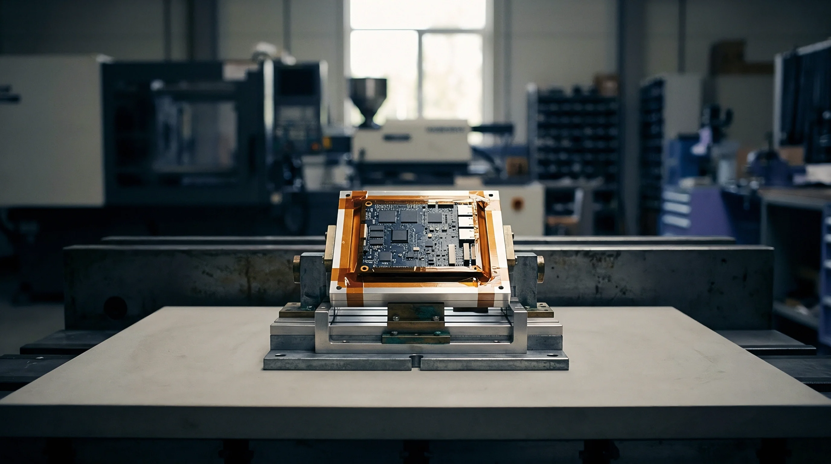
How Do File Formats Dictate Design Transfer Boundaries?
Exporting manufacturing documentation solely through static Gerber files restricts the buyer to basic fabrication while locking out netlist modifications. True design transfer requires complete native EDA databases alongside neutral exchange formats. The following step-by-step procedure establishes verification controls during design handover:
- Inspect incoming EDA repository files to verify readable schematic symbol libraries and intact signal netlists.
- Recompile the firmware source repository inside a clean build environment to ensure reproducible binary generation.
- Cross-check fabrication outputs against raw PCB layout databases to detect missing blind or buried via declarations.
- Audit bill-of-materials text exports against active distributor databases to identify single-sourced or end-of-life passive components.
Because Gerber files lack netlist intelligence, thorough verification ensures that second-source assembly houses can build functionally identical assemblies without engineering support from the originating factory.
An explicit intellectual property assignment clause specifying source code delivery within five working days prevents factory hold-ups during vendor transitions.


Jig
Automated factory test equipment enforces physical and functional compliance across high-volume production runs. Semicustom wireless modules demand customized fixture pin layouts to interface with RF test points, power rails, and programming pads. Designing, machining, and calibrating specialized test stations constitutes a major fraction of upfront non-recurring costs.
Test cycle duration inflates unit price directly through per-board manufacturing overhead on automated lines. Streamlining test routines while preserving defect coverage requires balancing fixture complexity against overall line throughput.

Automated Test Fixtures and RF Calibration
Pogo-pin test interfaces align with dedicated test pads on the printed circuit board to measure RF output power and frequency drift. Pneumatic clamping mechanisms apply uniform mechanical pressure to prevent signal loss across high-frequency contact probes. Because contact wear and sensor drift degrade log accuracy over time, fixture maintenance requires periodic replacement of worn pogo pins and recalibration of internal power sensors against reference standards.
| Test Scope | Upfront Fixture Cost ($) | Execution Time per Board (s) | Maintenance per 10k Units ($) | Primary Defect Addressed |
|---|---|---|---|---|
| Basic Continuity & Voltage | 4,500 | 3.5 | 250 | Solder Bridges & Open Traces |
| Conducted RF Power & Frequency | 18,000 | 8.0 | 1,200 | Matching Network Drift |
| Over-The-Air Radiation Pattern | 35,000 | 18.0 | 2,800 | Antenna Resonance Failure |
| Full Thermal Chamber Run | 62,000 | 120.0 | 5,500 | Crystal Frequency Drift |
Automated test equipment relies on golden units to anchor calibration, comparing live board measurements against reference modules verified under controlled laboratory conditions.

Yield Dynamics and Factory Test Capex
Defect rates during early factory bring-up directly increase per-unit processing expenses by occupying expensive test stations. When early manufacturing yields stumble, secondary rework labor quickly destroys projected bill-of-materials savings. Implementing rigorous test sequences early in the line prevents defective sub-assemblies from ever reaching enclosure integration.
- Initial Fixture Alignment Verification Misaligned mechanical contact pins damage printed circuit board gold pads, causing permanent board scrap.
- Golden Unit Reference Calibration Operating test stations without verified reference hardware produces systematic measurement offset errors across entire production batches.
- Automated Rework Routing Automated test logs failing boards directly to manual repair benches, preventing defective modules from entering final packaging lines.
Production test fixtures designed without secondary calibration loops report false yield passes during ambient thermal fluctuations.
Inadequate factory test coverage allows defective antenna matching networks to reach end customers, leading to field returns and brand damage.


Ledger
Balancing total product lifecycle expenditure demands ongoing evaluation of volume shifts, component price erosion, and field maintenance costs. Initial break-even calculations serve as static baseline models, but dynamic market conditions alter long-term economic returns. Supply chain volatility, component end-of-life notices, and changing regulatory standards shift financial returns over a multi-year manufacturing lifespan.
While unit cost drops with volume, re-masking silicon remains prohibitively expensive, so sourcing teams must continually audit landed costs to confirm that semicustom investments preserve their margin advantage over off-the-shelf modules.

Lifecycle Amortization and Volume Sensitivity
Product sales volumes falling short of original projections extend the timeline required to recover custom engineering charges. Sensitivity analysis models the effect of a 20 percent drop in annual unit shipments on non-recurring engineering recovery periods. When volume contracts, fixed test fixture capital expenses and regulatory filing fees are amortized over fewer units, eroding profit margins.
Conversely, volume expansions beyond original projections accelerate return on investment. Once production passes break-even thresholds, every shipped unit yields full bill-of-materials savings directly into gross product margin.

Second Source Switching Friction and Exit Costs
Transferring semicustom module manufacturing to an alternate facility involves secondary tooling expenses, factory audit delays, and regulatory re-filings. Exit costs include acquiring proprietary manufacturing test scripts, re-tooling shield stamping dies, and re-qualifying surface mount assembly lines. Buyers must calculate these potential transition costs when negotiating original manufacturing master service agreements.
Long-term commercial viable production requires continuous monitoring of component end-of-life notices to protect upfront engineering investments.