Meaning
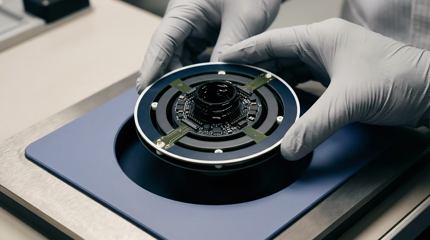
Electronic testing architectures defined by the IEEE 1149.1 standard enable structural verification of printed circuit boards by shifting data through specialized cells placed at the pins of integrated circuits. Logic cells known as boundary-scan cells reside between the internal device logic and each physical pin on the package. These specialized registers allow a tester to control or observe the electrical state of individual pins regardless of the internal logic state.
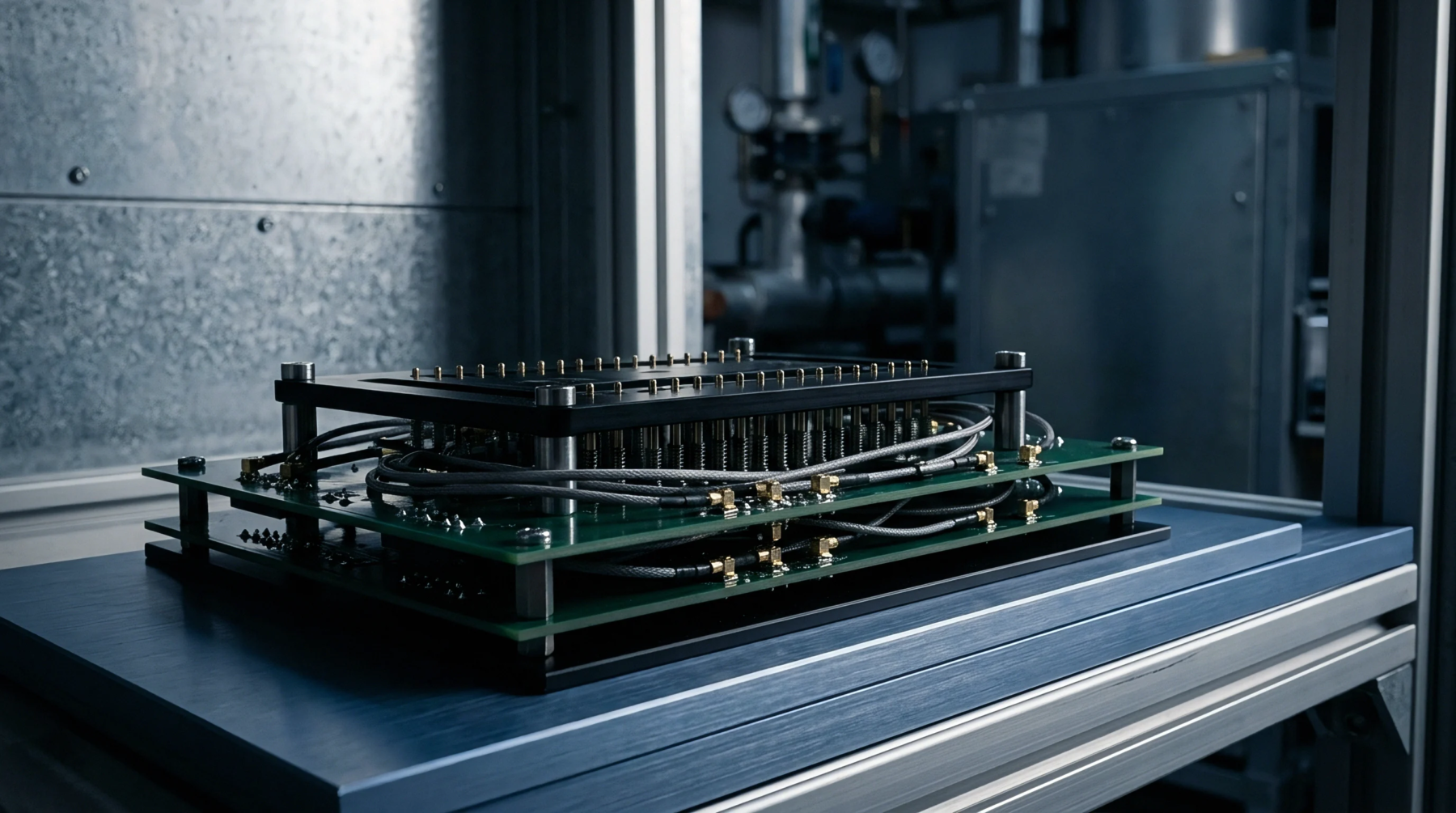
Using this method, engineers verify the integrity of solder joints and traces without using traditional physical test probes. It functions as a virtual bed of nails for modern surface mount technology where pins are hidden under component bodies. Integration of these cells into the silicon allows for non-destructive testing of high density assemblies.
Logic Architecture
Hardware implementations of the protocol require a minimum of four dedicated signals known as the test access port. Internal signals include the clock, mode select, data input, and data output lines which drive a state machine inside the silicon. The state machine controls whether the device is in a bypass mode, an identification mode, or a mode that captures pin data.
Boundary-scan relies on these internal instructions to determine which registers are connected between the data input and output. Designers include a boundary scan description language file to tell the testing software how the internal cells are mapped to physical pins. The instruction register holds the current command while the data registers hold the actual bit patterns.
Interconnect Validation
Automated test equipment uses the shift registers to drive specific logic patterns across the board traces. In a typical sequence, one chip drives a high signal on a specific pin while a receiving chip captures the state at the other end of the trace. If the receiving chip sees a low signal, the software identifies an open circuit in the signal path.
This process detects solder bridges between adjacent pins by driving alternating patterns of ones and zeros across the bus. Because boundary-scan does not require the board to be powered up in a functional state, it identifies assembly errors before full power is applied. This capability prevents damage to expensive components caused by short circuits on the power rails.
Verification software compares the captured vectors against the board netlist to ensure every connection is correct.
Fault Isolation
Software algorithms analyze the results of the scan to provide the exact location of electrical faults on the assembly. When a test fails, the diagnostic report names the specific net and the associated pins that did not match the expected vector. This precision reduces the time spent on manual debugging and allows technicians to go straight to the rework station.
Boundary-scan provides a reliable way to check connections under ball grid array packages where pins are not visible to the eye. It supports the debugging of prototypes by allowing engineers to force signals into a processor to verify peripheral operation. The method remains effective throughout the product life from initial prototyping to high volume manufacturing.