Managing Asynchronous Silicon Errata and Firmware Abstraction Protocols across Alternate Hardware Manufacturing Sites
Dynamic firmware abstraction protocols and standardized test jigs eliminate operational failures caused by asynchronous silicon errata across alternate factories.

Register
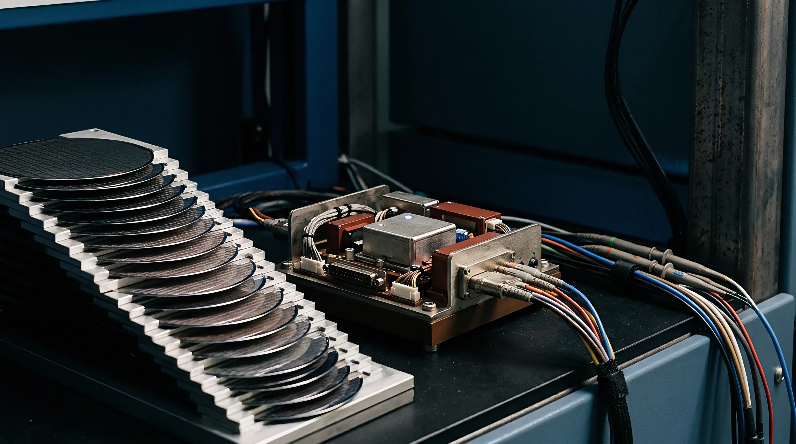
Silicon dies sourced from split foundry allocations or staggered lithography runs present distinct electrical and logic deviations despite carrying matching part numbers. Wafer fabrication plants adjust planar dopant profiles, replace worn reticles, or modify metal deposition rates to recover yield on aging production nodes. These process variations alter propagation delays across internal interconnect matrices, yielding asynchronous timing violations in peripheral logic buses.
When a microcontroller or radio transceiver fabricated at a primary plant in Taiwan encounters a second source fabrication run at a facility in Singapore, internal silicon timing closures drift. Peripheral status flags fail to assert within expected clock boundaries, and shared Direct Memory Access channels corrupt transmission buffers during high-speed serial bus transfers.
Microcode revisions inside monolithic silicon systematically fail to expose these timing anomalies through basic vendor datasheet summaries. Silicon revisions introduce register anomalies. Hardware designers who mirror vendor evaluation board layouts without accounting for foundry-specific errata sheets invite critical operational faults during high-volume production transfers.
Foundries issue engineering change notices with alphanumeric errata indexes, yet these revisions arrive months after distribution pipelines disperse mixed die revisions across global distributors. Sourcing teams receiving reels with mixed date codes unknowingly place disparate stepping revisions onto identical assembly lines.
A firmware driver that polls a peripheral status register without bounded timeout escapes locks execution during cold-boot states when gate oxide thickness shifts between semiconductor foundries.
Peripheral register anomalies surface under distinct clock boundary crossings. Alternate foundries run distinct fab recipes. An integrated Universal Asynchronous Receiver-Transmitter or Serial Peripheral Interface controller operates through internal synchronizer flip-flops designed to resolve metastability.
A marginal change in threshold voltage between foundry processes pushes setup and hold times outside design tolerances. The peripheral controller drops the final byte of an incoming frame or generates a phantom parity error. SCM and I2C interfaces display analog rise-time sensitivities where differing output pad driver strengths cause bus arbitration deadlocks on the physical wiring.

Foundry Recipe Variations and Logic Deviations
Semiconductor foundries balance process design kits against their specific equipment fleets, causing measurable deviations across identical intellectual property blocks. Gate oxide thickness variations alter static leakage currents and baseline transconductance parameters. When an alternate production site uses an older steppers system, metal line edge roughness increases parasitic capacitance across adjacent traces within the integrated circuit logic array.
These capacitive spikes skew the propagation delay of internal reset lines, exposing race conditions inside asynchronous state machines that the initial design verification suite missed.
| Silicon Stepping | Fabrication Facility | Lithography Node | Hardware Fault Mechanism | Observed Failure Mode |
|---|---|---|---|---|
| Revision A0 | Hsinchu Fab 12 | 40 nm LP | DMA request synchronizer setup violation | Buffer overrun during SPI transfers above 24 MHz |
| Revision A1 | Tainan Fab 14 | 40 nm eFlash | Internal charge pump voltage ripple | Brownout reset trips during flash write sequences at -20 C |
| Revision B0 | Dresden Fab 1 | 40 nm RF-CMOS | Output buffer slew rate mismatch | I2C clock stretching failure under multi-master arbitration |
| Revision B2 | Singapore Fab 7 | 40 nm LP | Asynchronous timer prescaler gate race | Missed capture interrupt on high-frequency PWM inputs |
Design teams mitigate these discrepancies by validating silicon registers against hardware test patterns rather than vendor behavioral simulators. Oscilloscope probes placed on bus clock lines and chip-select strobes expose ringback voltages caused by higher output drive impedances on second-source silicon. When production runs mix Revision A1 and Revision B0 dies, firmware written to clear interrupt flags through simple write-one-to-clear operations fails on the later revision due to pipelined bus bridges delaying the bus write completion.
The interrupt service routine exits before the hardware register clears, retriggering the interrupt handler indefinitely and halting system execution.
The vendor representative explained that the silicon errata fell entirely within published electrical specifications and that customer firmware should incorporate software delays around peripheral status register reads.


Pin
Physical packages housing split-lot silicon dies demonstrate mechanical and inductive shifts that degrade signal integrity across alternate printed circuit board assembly facilities. Assembly and test contractors employ varied wire-bonding metallurgical compositions, switching between pure gold, copper, and palladium-coated copper wire bonds to control material expenses. A change in bonding wire material shifts the parasitic lead inductance by up to four nanohenries on high-speed input and output terminals.
Alternate contract manufacturing lines in mainland China and Malaysia also deploy divergent surface-mount technology reflow profiles, creating localized voiding under bottom-termination components such as Quad Flat No-Lead packages.
Ground bounce elevates logical low thresholds above acceptable operational margins during synchronous switching events. Voltage drops trigger brownout resets. When thirty-two input and output pins switch simultaneously on a high-density package, the parasitic inductance in the ground bond wires induces a transient voltage spike across the internal die substrate.
If the secondary packaging facility utilizes longer bond wires or thinner die-attach epoxy to compensate for alternative lead-frame tooling, the peak ground bounce voltage doubles, inducing false low-to-high transitions on adjacent static interrupt lines.

Physical Packaging Divergence across Assembly Plants
Packaging facilities utilize varying mold compound formulations with disparate dielectric constants and thermal expansion coefficients. A higher dielectric constant increases pin-to-pin parasitic capacitance, distorting edge rates on high-speed memory interfaces such as Octal-SPI and Quad-SPI. Package substrates warp unevenly across secondary reflow passes when automated optical inspection parameters fail to catch uneven solder paste volumes beneath thermal center pads.
The absence of solid thermal conductivity raises silicon junction temperatures during extended duty cycles, shifting internal clock oscillator calibrations beyond the lock ranges of phase-locked loop circuits.
- Package Lead Inductance shifts signal rise times and induces ground bounce during simultaneous switching output cycles on unshielded digital interfaces.
- Bond Wire Metallurgy alters internal resistance profiles and creates localized thermal throttling during continuous radio frequency transmissions.
- Center Ground Voiding reduces heat dissipation efficiency and destabilizes radio frequency low-noise amplifier bias points under sustained operational loads.
- Solder Mask Thickness shifts radio frequency trace impedance across high-frequency coplanar waveguide sections on peripheral interface lines.
Automated manufacturing audits require precise verification of component lot traceability records down to individual reel splices. Solder mask thickness shifts impedance. Second sources introduce clock jitter.
When alternate assembly lines swap assembly chemicals without informing the procurement authority, flux residue left under low-standoff packages forms conductive dendritic pathways under humid operating conditions. These micro-bridges alter the pull-up resistance on critical hardware configuration strapping lines, causing the microcontroller to boot into factory test modes rather than standard application runtimes.
Overlooking package-level inductance deviations and solder joint geometry shifts during alternate site qualification generates catastrophic field returns when automated assembly processes produce thousands of units with marginal timing margins that fail under temperature extremes.


Abstraction
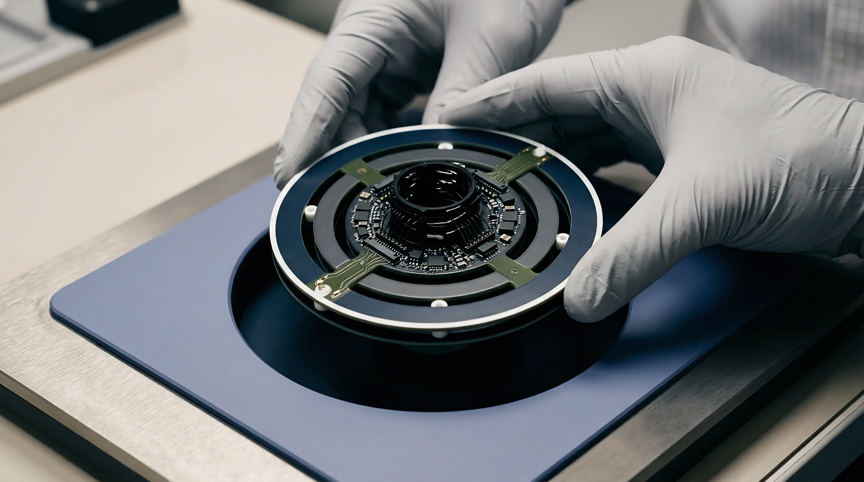
Hardware isolation protocols separate hardware-dependent register accesses from core business logic through structured driver translation layers. A robust software architecture incorporates dynamic hardware revision detection routines at system boot, inspecting hardware register identifiers and silicon stepping fuses before initializing peripheral device drivers. Rather than compiling separate binary images for each silicon revision, a single unified firmware binary queries system hardware identifiers, dynamically dispatching function pointers to target-specific peripheral routines.
This structure accommodates asynchronous silicon errata without requiring alterations to high-level application code.
Patch tables reside in flash sectors. When a system boots, the reset handler reads the electronic chip identification registers located at predefined read-only memory addresses. The firmware cross-references these hardware registers against an internal lookup table containing active silicon errata workarounds.
If the lookup confirms Revision A0 silicon from a specific fab, the abstraction layer routes serial peripheral driver calls to an execution path that executes software-managed clock gating, preventing the hardware DMA synchronizer setup violation from corrupting payload buffers.
A compiled binary containing dynamic errata dispatch logic increases flash memory allocation by 14.8 kilobytes compared to a static vendor reference driver on a Cortex-M4 microcontroller.
Execution latency increases when function pointers replace direct register writes in performance-critical control loops. Hardware abstraction isolates peripheral variances. To mitigate this penalty, the abstraction layer provides hardware abstraction routines that compile into static inline functions when firmware targets a dedicated, single-source hardware build.
In multi-source deployments, the firmware trades minor latency increments for operational stability across split manufacturing batches, executing patched peripheral read cycles that guarantee bus idle states between successive read-modify-write transactions.
Software Protocol Implementation for Silicon Errata Isolation
Vendor software development kits rarely provide modular structures for managing mixed silicon steppings in high-volume production. Reference drivers provided by semiconductor vendors frequently employ blocking busy-wait loops that lock up microcontrollers when silicon logic fails to clear status flags due to unexpected hardware state machine hangs. Embedded engineering teams write custom hardware abstraction protocols that encapsulate register interactions within time-bounded polling structures, pairing each status check with a hardware timer fallback mechanism.
| Protocol Layer Model | Memory Footprint | Execution Overhead | Silicon Errata Agility | Portability Across Factories |
|---|---|---|---|---|
| Vendor Static Library | Minimal (8 KB) | Negligible (Direct I/O) | Zero (Requires Recompilation) | Low (Coupled to single die stepping) |
| Dynamic Jump Table | Moderate (24 KB) | Low (3 to 5 clock cycles per call) | High (Runtime die detection) | High (Unified binary across all fabs) |
| Inline Wrapper Architecture | Low (12 KB) | Very Low (1 to 2 clock cycles) | Moderate (Build-time macro flags) | Moderate (Separate binaries per site) |
| Full Hardware Abstraction Service | High (64 KB) | Moderate (Context switch penalty) | Maximum (Complete virtualization) | Maximum (Hardware independent) |
Memory allocations within the dynamic abstraction layer accommodate flash patch tables. Flash memory cycles slow boot time. When second-source microcontrollers exhibit erratic analog-to-digital converter linearity due to silicon bandgap reference drift, the abstraction protocol applies factory calibration offset vectors stored inside non-volatile configuration memory.
During the manufacturing test sequence, bed-of-nails test fixtures calculate these offset factors and burn them into customer-programmable flash sectors, enabling the runtime abstraction layer to linearize sensor telemetry without modifying downstream analytical routines.
Unified binary images supporting runtime dispatch scale cleanly across alternate production facilities, while site-specific firmware builds inevitably cause field flashing failures when factory logistics mix finished inventory batches.


Jig
Automated manufacturing test fixtures maintain product consistency across distributed manufacturing locations by enforcing identical functional verification gates. Contract manufacturing sites in differing geographical locations often run disparate test instrumentation, ranging from legacy automated test equipment to modern modular instrumentation based on PXI backplanes. A robust qualification protocol mandates that all alternate manufacturing sites utilize standardized functional test jigs running identical firmware images, bed-of-nails spring contact pin interfaces, and calibrated signal measurement blocks.
Inspection cameras miss solder voids. Trace capacitance delays clock edges. When an alternate production site assembles printed circuit boards, the factory test fixture verifies that the board-level hardware responds correctly to boundary-scan instructions and peripheral functional checks.
The functional tester executes diagnostic firmware loaded into internal static random-access memory, testing peripheral interfaces at extreme operational frequencies and voltages to surface timing marginalities linked to silicon errata before the product leaves the manufacturing floor.

Secondary SMT Site Functional Calibration
Test fixture calibration parameters drift under continuous mechanical cycling on high-throughput surface mount assembly lines. Fixture relays degrade contact resistance. Spring-loaded pogo pins accumulate chemical flux residues and oxidation, increasing resistance between the measurement hardware and target test pads.
If a secondary assembly plant fails to implement a daily fixture verification routine, false passes occur where marginal silicon packages clear quality checkpoints because the fixture fails to exercise high-speed peripheral bus timing limits.
- Fixture Golden Unit Verification executes every twenty-four hours using designated calibration boards to confirm baseline measurement drift across analog channels.
- Boundary Scan Structural Checks validate pin continuity and detect cold solder joints beneath ball grid array packages before powering high-current rails.
- High-Speed Bus Stress Sweeps inject clock jitter and alter supply voltages by five percent to force timing-marginal silicon into detectable state-machine faults.
- Dynamic Errata Register Assertion reads electronic chip IDs and confirms that embedded firmware accurately executes the correct runtime workaround routines.
Engineering change notices governing manufacturing test packages dictate precise hardware revision thresholds. Build flags isolate silicon revisions. The test jig architecture logs every device serial number alongside its read-out electronic silicon identification register, packaging date code, and measured electrical margins.
SMT site operators must not modify test script timeout parameters or bypass peripheral stress tests to improve first-pass yield metrics. When production lines in alternate facilities record divergent yield curves on identical silicon lots, the discrepancy points directly to fixture wiring variance or improper thermal control during the reflow process.
Under IPC-9252 guidelines for electrical testing, unverified modifications to test pad contact resistances or fixture wiring invalidate the production acceptance certificate.
Under Section 6.2 of the typical Master Manufacturing Agreement, any alteration to automated test scripts or fixture schematics executed by an assembly contractor without prior written customer authorization constitutes a material breach that invalidates product warranties and places financial liability for field failures entirely on the contract manufacturer.


Dossier
A comprehensive design transfer dossier governs the technical transfer of electronic designs between alternate production sites without risking intellectual property contamination or manufacturing discrepancies. The dossier defines the boundary between buyer-owned assets and factory-owned tooling. Sourcing teams assembling this package deliver native computer-aided design files, complete fabrication schematics, full bill of materials databases with approved vendor lists, calibrated Gerber fabrication outputs, and containerized firmware build environments.
Without an audited transfer dossier, alternate manufacturing lines deploy substituted passive components that shift high-speed impedance matching networks, exacerbating silicon-level peripheral timing errata.
Assembly lines shift thermal profiles. Sourcing agreements define who pays for the non-recurring engineering fees required to modify firmware abstraction protocols when primary silicon foundries cease production of an approved die revision. When a semiconductor vendor issues a product discontinuation notice or shifts fabrication to an alternate facility, engineering hours mount quickly.
The engineering scope document specifies whether the contract manufacturer or the buyer bears the cost of rewriting peripheral drivers, designing new bed-of-nails functional test fixtures, and obtaining updated regulatory certifications.

Scope Division and Commercial Ownership Models
Turnkey manufacturing arrangements frequently mask intellectual property lock-in behind lower upfront non-recurring engineering costs. In a pure turnkey model, the original design manufacturer retains ownership of the board layout databases, firmware source code, and automated test scripts, providing the buyer solely with compiled binary files and finished goods. When component shortages force a transition to an alternate assembly house, the buyer finds themselves unable to execute a transfer because they lack the low-level firmware abstraction source code required to adapt to alternative silicon steppings.
Semi-custom agreements address this vulnerability by explicitly assigning ownership of firmware source repositories, hardware schematics, and functional test software to the buyer upon completion of milestone payments. Sourcing agreements stipulate that all board support packages, peripheral abstraction layers, and factory calibration routines must compile through reproducible, containerized build scripts that do not depend on proprietary vendor toolchains. The engineering fee structure separates initial board bring-up costs from ongoing maintenance fees, establishing fixed hourly billing rates for qualifying alternate silicon revisions.
Part-change notification agreements require semiconductor suppliers and contract manufacturers to provide a minimum of ninety days advance written notice prior to introducing alternative silicon steppings, packaging materials, or assembly line relocations. This window allows integration engineers to run comprehensive electrical qualification tests, update dynamic errata lookup tables, and validate test fixture scripts across secondary facilities before mass production ramps. Failure to secure contractual enforcement of part-change notification timelines leaves purchasing teams vulnerable to silent silicon migrations that destabilize field reliability.
What remains unresolved across modern multi-source manufacturing operations is whether unified hardware abstraction layers can dynamically neutralize unforeseen analog silicon errata without requiring costly physical board redesigns or manual factory recalibrations.