Meaning
An electrical phenomenon occurs when high currents pass through the parasitic inductance of a ground pin, causing the local reference voltage of a chip to momentarily rise above zero. This shift disrupts the logic thresholds of sensitive data signals and can lead to unwanted logic transitions or system crashes. Ground bounce results from the interaction between the speed of digital switching and the mechanical constraints of the package leads.
When thousands of tiny transistors switch simultaneously inside a microprocessor, the total demand for current creates a measurable spike across any resistive or inductive bottleneck. The limit of this effect is reached when the reference voltage moves enough to trigger a false high signal on a neighboring idle pin. It remains a critical concern for engineers working on high frequency modules and dense logic boards.
Package Parasitics
Lengthy bond wires and lead frames within an integrated circuit enclosure contribute the most to the total inductive path. Minimizing ground bounce requires selecting components with very short paths between the silicon die and the printed circuit board ground plane. Devices with multiple ground pins help by spreading the current across several parallel inductive paths, effectively reducing the overall voltage drop.
Designers often choose ball grid array packages for this reason because they offer shorter paths compared to quad flat pack variants. The physical interface of the pins directly determines how much voltage displacement will occur during a high throughput data cycle. Reducing the length of these connections is essential for signal integrity in modern hardware.
Board Layout
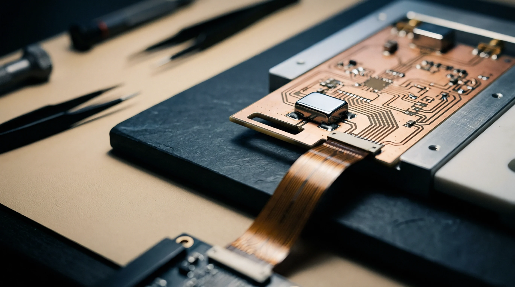
Routing decisions made on the mother board can either amplify or dampen the noise generated inside the silicon. Mitigation of ground bounce involves placing a large reference plane directly beneath the high speed component to offer the lowest possible return impedance. Gaps in the ground plane or long narrow traces to the via destroy the stability of the local zero volt reference.
High frequency decoupling capacitors are also used to keep current local, though their effectiveness depends on the distance between the part and the chip. If multiple chips share a poor ground path, one active device can trigger errors in its quiet neighbor through mutual inductance. Every milliohm of resistance in the ground network makes the reference more vulnerable to these transient shifts.
System Consequences
Failures related to this phenomenon are often difficult to diagnose because they manifest as intermittent logic errors or sporadic memory data corruption. High levels of ground bounce can lower the effective signal to noise ratio of communication lines, increasing the bit error rate. In some cases, the voltage rise is sufficient to trigger the protection diodes of an input port, which might latch the system into an unrecoverable state.
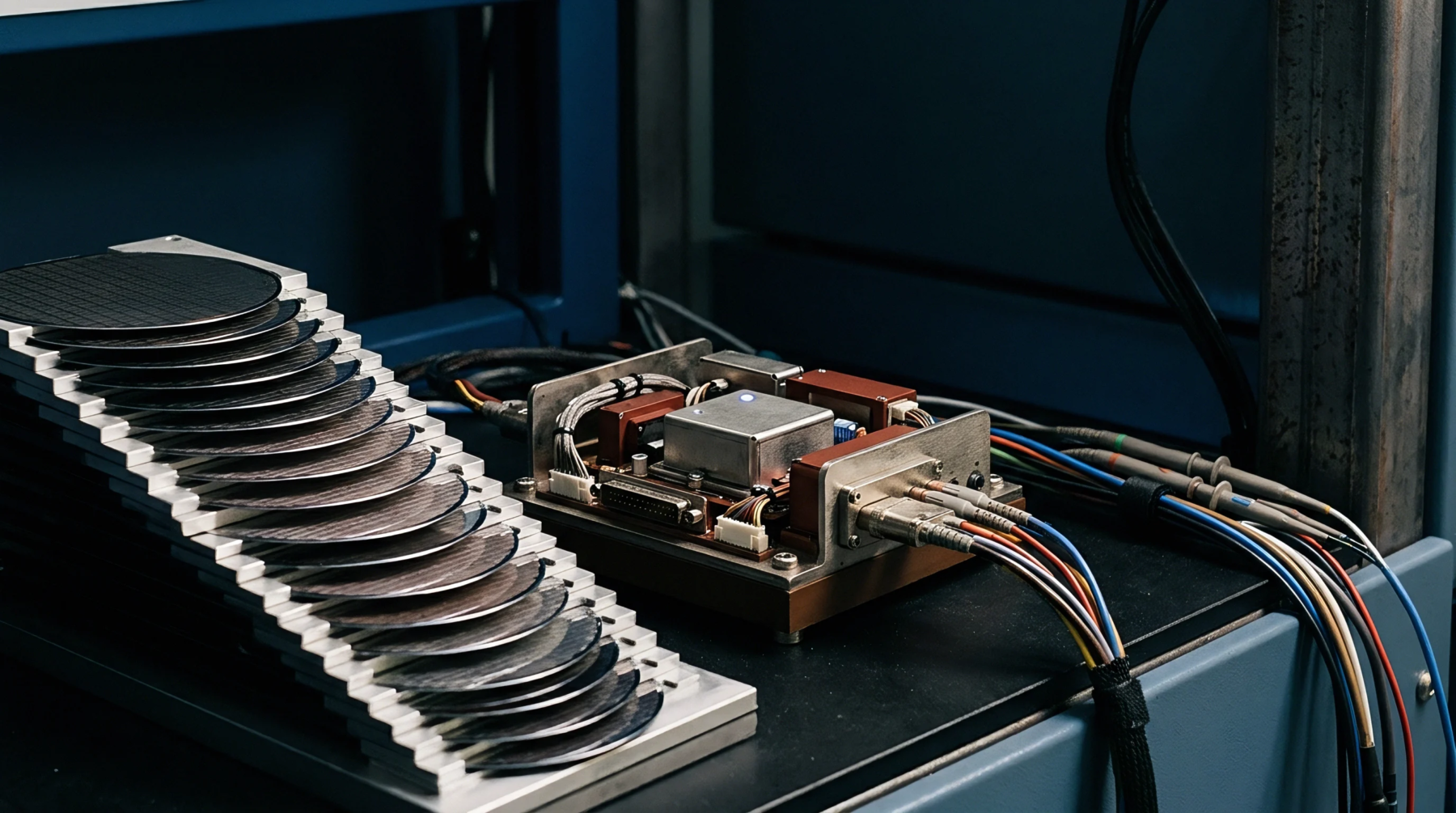
Verification involves using high bandwidth oscilloscopes to probe local pins during stress tests that simulate full load operation. These test sequences reveal if the board fit is sufficient for the thermal and electrical budget of the high performance components. Solving these errors late in the production cycle often leads to significant cost increases and delays.