Quartz Crystal Drive Level Dependency under High Transmit Current Bursts
High transmit current bursts shift crystal drive levels, causing motional resistance jumps and frequency pulling that degrade wireless packet transmission.
Mechanics
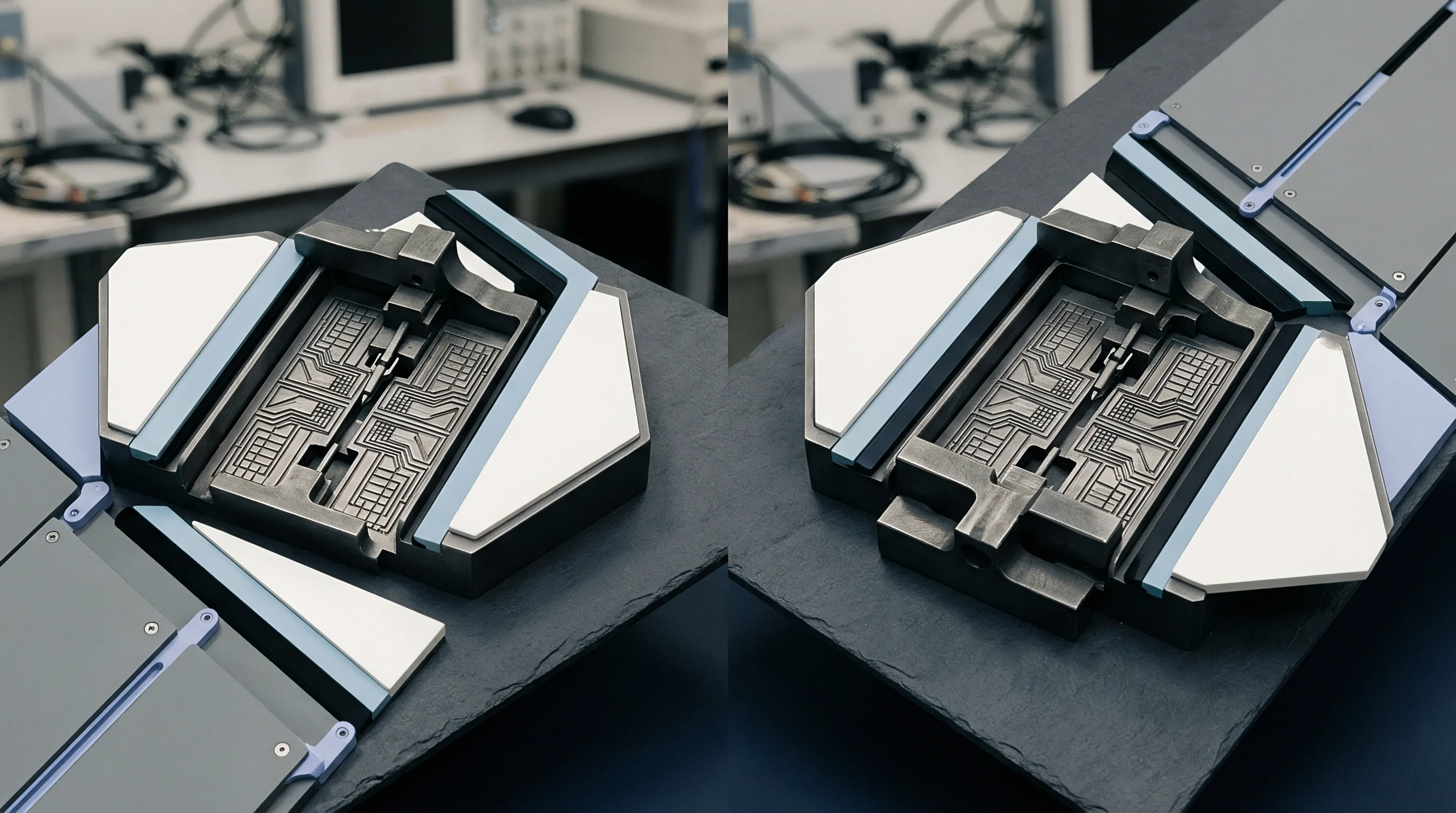
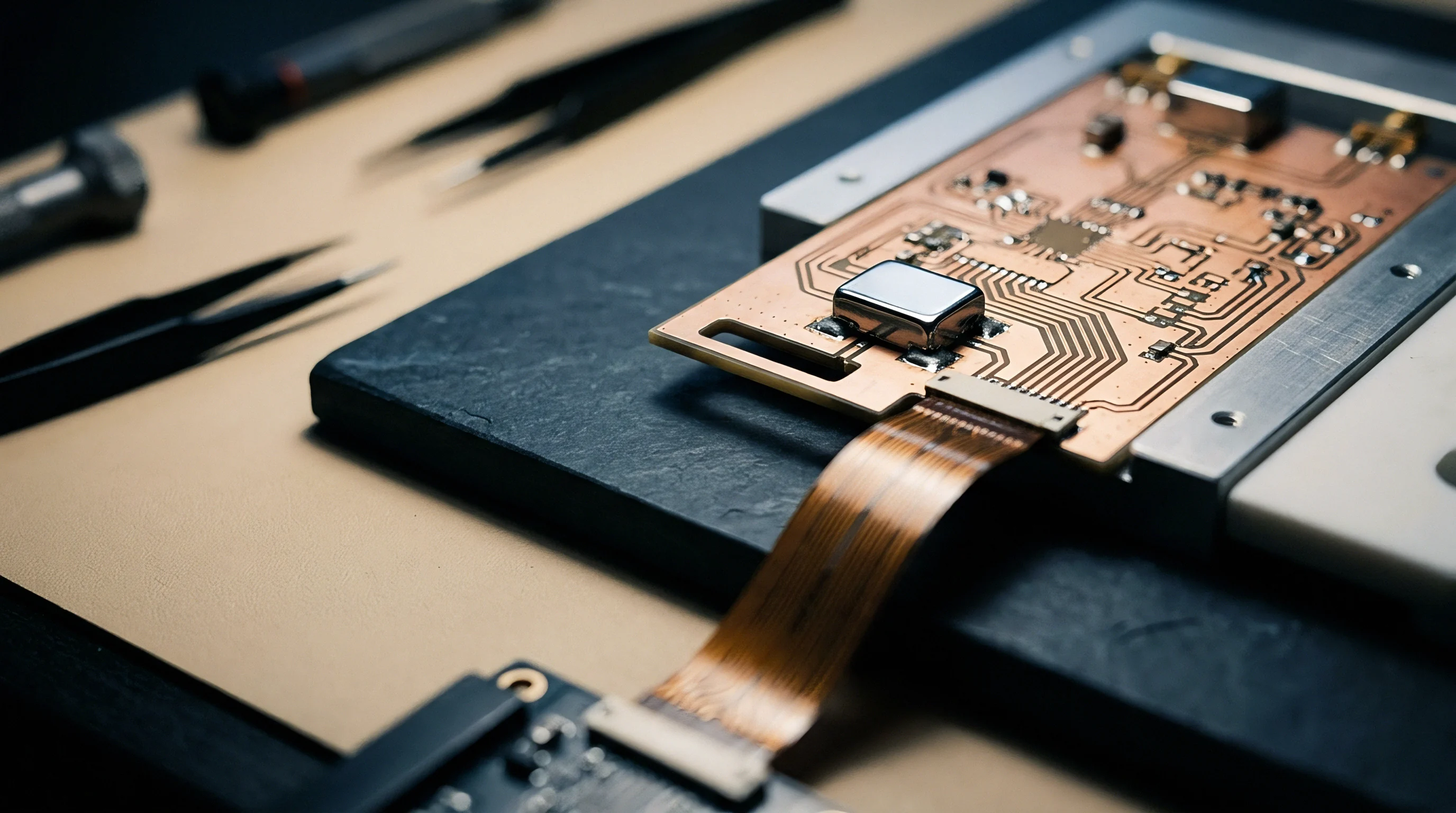
Oscillating quartz crystals rely on acoustic standing waves set up inside a micro-machined AT-cut quartz blank. As an electromechanical transducer, mechanical stress generates electric polarization across the crystal while an applied voltage creates physical strain. In a quiet state, the microcontroller or RFIC Pierce oscillator drives the blank within its linear region, keeping motional resistance (R1) stable and resonant frequency fr fixed.
Drive levels inside standard low-power wireless nodes usually hover between 10,μW and 100,μW.
Transmitting breaks this baseline. As the radio ramps output power from a low-power listening state to maximum burst, power amplifiers draw heavy current that triggers fast electrical and thermal transients across the board. Peak current spikes in LTE-M and NB-IoT modules routinely reach 500 mA to 2 A within microseconds, while Wi-Fi 6 transceivers and high-power LoRaWAN nodes pull 120 mA to 500 mA during active frames.
These current surges perturb the reference quartz crystal through several coupled physical channels.
Transmit Burst Coupling
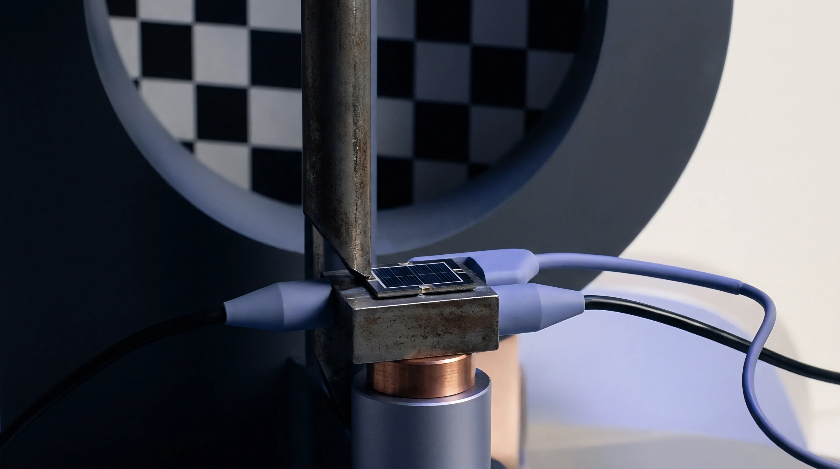
When the power amplifier turns on, it pulls current from the supply network almost instantaneously. This steep dI/dt causes transient IR drops across PCB trace resistances and parasitic inductances, sagging the supply rail and shifting bias on the oscillator’s internal inverter. To compensate for lower headroom, automatic gain control circuits or transconductance stages boost drive current into the crystal.
Ground bounce also shifts the reference point for the crystal load capacitors. As high transmit currents push the local ground plane around, peak-to-peak voltage across the crystal terminals widens, driving current past safe limits. Dissipated power in the quartz blank then climbs above the linear operating threshold, pushing the resonator into non-linear drive level dependency.
Drive Level Non-Linearity
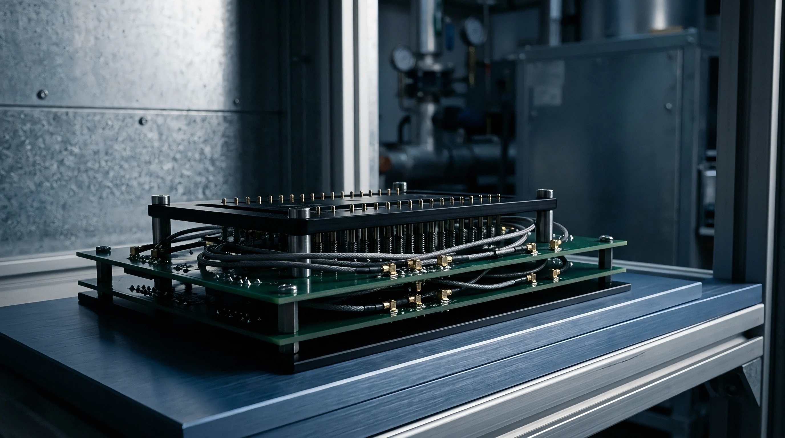
Below five microwatts, micro-defects on the crystal electrode surface elevate motional resistance. As drive power enters the normal operating band, resistance drops to its minimum. But when power surges past a hundred microwatts during a transmit burst, stress in the quartz lattice engages non-linear elastic constants that cause motional resistance to spike.
This variation in equivalent series resistance (R1) is known as Drive Level Dependency (DLD). A crystal that measures a clean 30,Ω under quiet bench conditions can jump above 120,Ω when over-driven during an RF pulse. If sustaining transconductance (gm) in the Pierce oscillator cannot handle the sudden resistance jump, loop gain drops below unity and the oscillator stalls.
More commonly, the non-linear drive pulls the mechanical resonant frequency, shifting carrier frequency right in the middle of the packet.
- Motional Resistance Jump reduces loop gain margin, extending start-up times or dropping oscillation entirely during high-power bursts.
- Frequency Pulling Effect pulls fundamental resonance by tens of ppm as internal mechanical strain alters acoustic wave velocity across the quartz.
- Thermal Dissipation Gradient creates localized heating inside the crystal package, adding secondary thermal frequency drift on long packets.
- Subharmonic Spurious Modes trigger when high drive levels couple energy into unwanted mechanical modes, raising phase noise and jitter.
The interaction between dynamic power amplifier current and quartz resonator performance varies systematically across physical drive regimes.
| Drive Power Range (μW) | Motional Resistance R1 (Ω) | Resonant Frequency Shift (ppm) | Physical Failure Mode Under Burst Load |
|---|---|---|---|
| 0.01 to 1.0 | 60 to 180 | +5 to +15 | Oscillator start-up failure due to high initial resistance from surface micro-defects. |
| 1.0 to 100 | 20 to 35 | -1 to +1 | Nominal linear operating zone with stable phase noise and predictable loop margin. |
| 100 to 300 | 35 to 75 | -5 to -12 | Non-linear lattice strain causing carrier frequency offset during active frame transmission. |
| 300 to 1000 | 75 to 220+ | -12 to -35+ | Thermal stress and mode coupling leading to EVM breakdown or total oscillation quenching. |
Drive level frequency offsets during current pulses fall outside standard warranty conditions when operating power exceeds nominal micro-watt limits.


Impairment
Wireless standards require tight frequency stability throughout packet delivery to preserve channel spacing and satisfy error vector magnitude limits. When transmit current spikes push the reference crystal into its drive level dependency zone, the resulting carrier offset directly degrades physical layer performance.
As crystal motional parameters shift, phase noise spikes sharply and disrupts the PLL synthesizer tracking loop. Since the reference oscillator sets the baseline for the local oscillator, any frequency shift at the crystal multiplies up to sub-GHz or 2.4 GHz bands, turning tiny fractional resonance changes into significant carrier offsets.
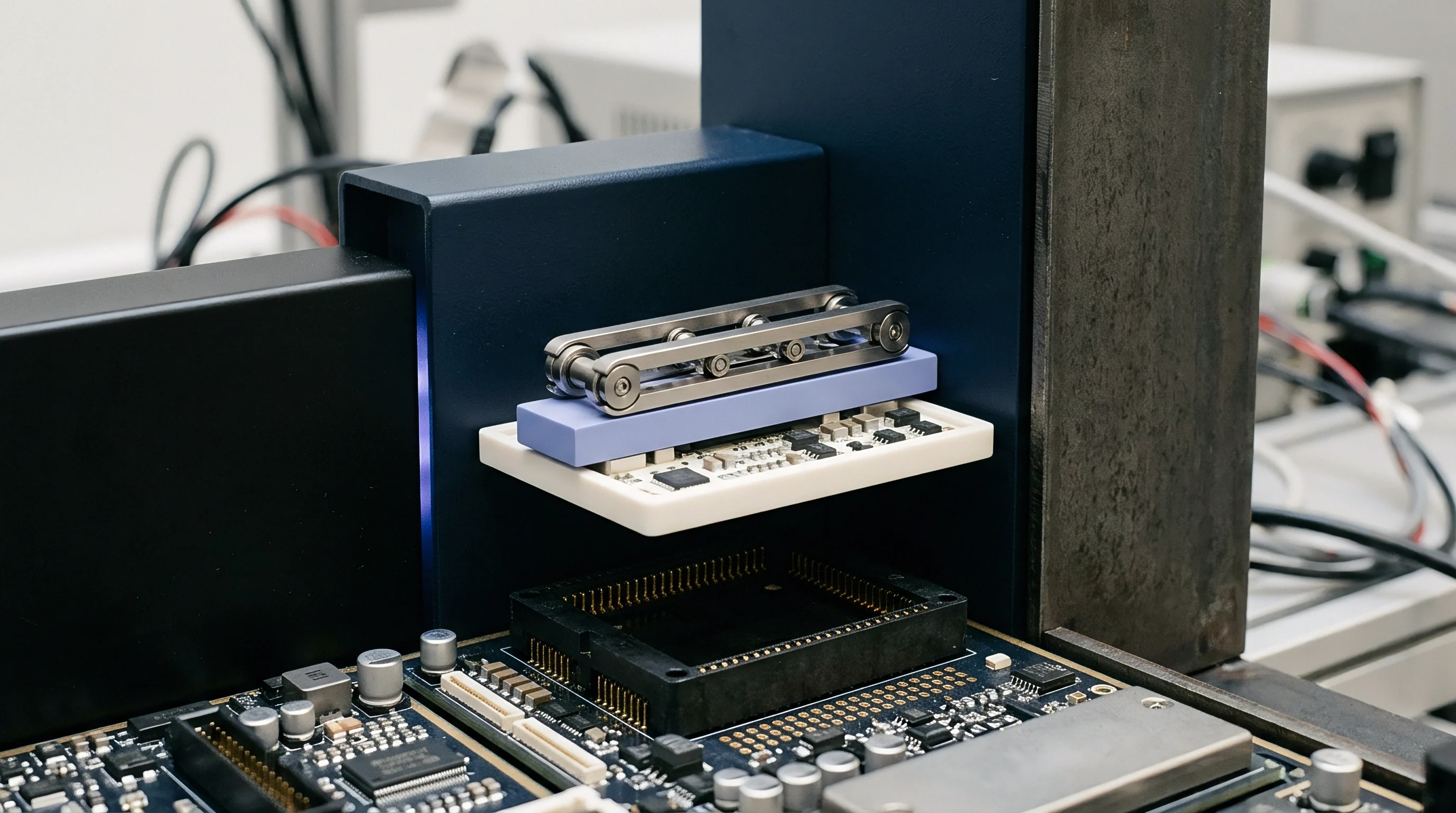
Carrier Frequency Offset in Cellular IoT
LTE-M and NB-IoT modems rely on narrow 15 kHz subcarriers, with single-tone NB-IoT dropping down to 3.75 kHz. Pushing 23 dBm of transmit power pulls heavy peak current from the battery, inducing supply droop and heating components near the crystal.
If drive level dependency shifts a 900 MHz reference by 10 ppm, carrier offset reaches 9 kHz ~ well beyond the subcarrier channel bandwidth. Subcarrier alignment degrades, forcing the base station eNodeB to lose phase lock and generate block errors. Once frame synchronization fails, the modem drops off the network and must execute a full re-attach cycle that wastes far more energy than the original transmission.
A carrier frequency deviation exceeding 2.5 ppm during an LTE-M transmission at 23 dBm output power elevates packet error rates above eight percent in poor link budget conditions.

Spectral Splatter and Error Vector Magnitude
Wideband digital formats depend on phase stability across the full packet length. Wi-Fi 6 (802.11ax) uses 1024-QAM constellations that demand EVM below -35 dB, while LoRaWAN uses Chirp Spread Spectrum where timing accuracy sets chirp linearity.
When current bursts alter crystal series resistance mid-frame, step changes in phase create transient splatter into adjacent channels, causing selectivity to fall off. In LoRaWAN links, the resulting chirp slope distortion degrades processing gain at the gateway, pulling line-of-sight range down from 15 kilometers to under two kilometers for the same link margin.
In a 2.4 GHz IEEE 802.15.4 Zigbee transmitter delivering 20 dBm over a 4 ms burst, the power amplifier draws 180 mA from a regulated 3.3 V rail. That load induces a 45 mV ripple at the switcher frequency, modulating the driver transconductance and pushing crystal power from 50,μW to 280,μW. Motional resistance rises from 25,Ω to 85,Ω, introducing an 8 ppm carrier shift during the frame header.
Demodulators experience phase error acceleration across the payload. Elevated phase noise from the reference drops sensitivity from -102 dBm to -88 dBm, killing the packet before completion.
Ignoring burst-induced frequency pulling leads to excessive retransmissions, reduced throughput, and early battery failure across IoT deployments.

Strain
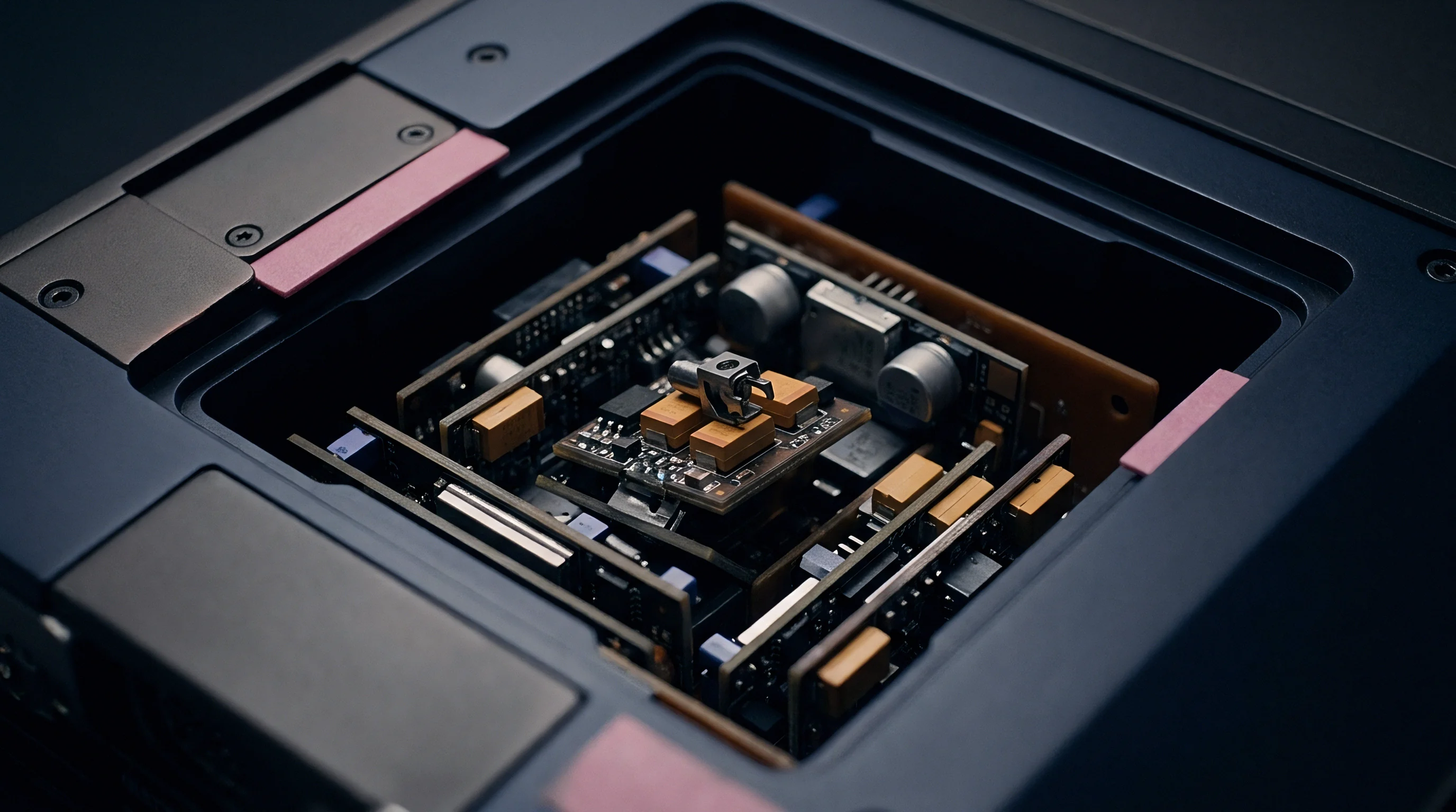
Heat generated by the power amplifier flows quickly into neighboring PCB copper traces. Because copper is highly conductive, thermal energy reaches surrounding passives within milliseconds. Crystal packages placed close to the RFIC to keep traces short end up directly in this heat path.
Mechanical strain accompanies these thermal shifts. High current transients through decoupling inductors generate localized magnetostriction, while fast thermal expansion of the glass-epoxy board puts shear stress on ceramic package pads, physically flexing the quartz blank inside.
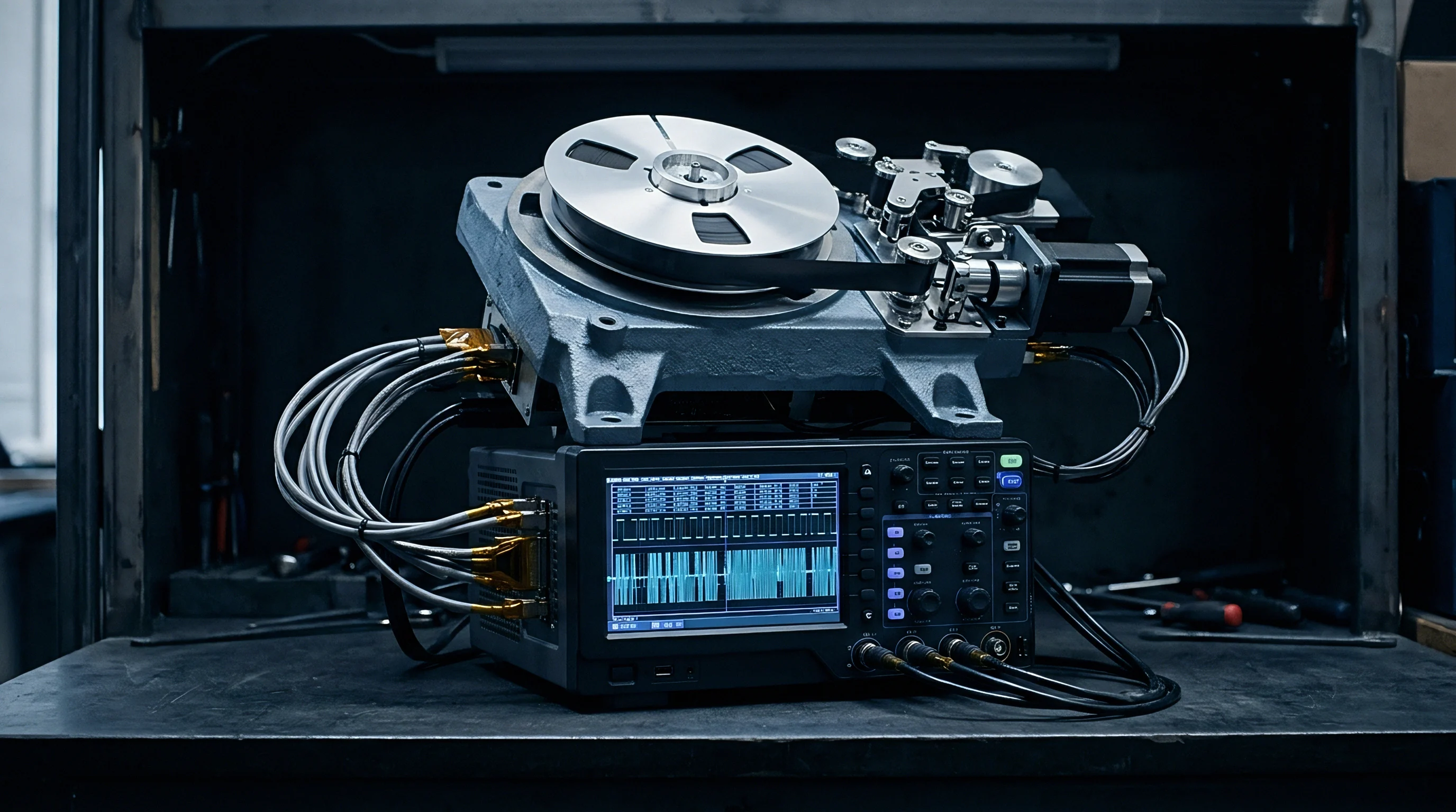
Thermal Diffusion and Gradient Profiles
Heat from a transmit pulse diffuses through board layers according to copper weight and substrate conductivity. The mismatch in thermal expansion coefficient between the ceramic enclosure (6.5 × 10⁻⁶/K) and FR4 board (14 × 10-6/K) exerts mechanical force directly across the solder joints.
Lattice strain alters resonant frequency independent of uniform ambient temperature shifts. While ambient temperature changes follow predictable parabolic curves defined by the AT-cut angle, transient mechanical stress creates asymmetrical frequency drift during transmissions.
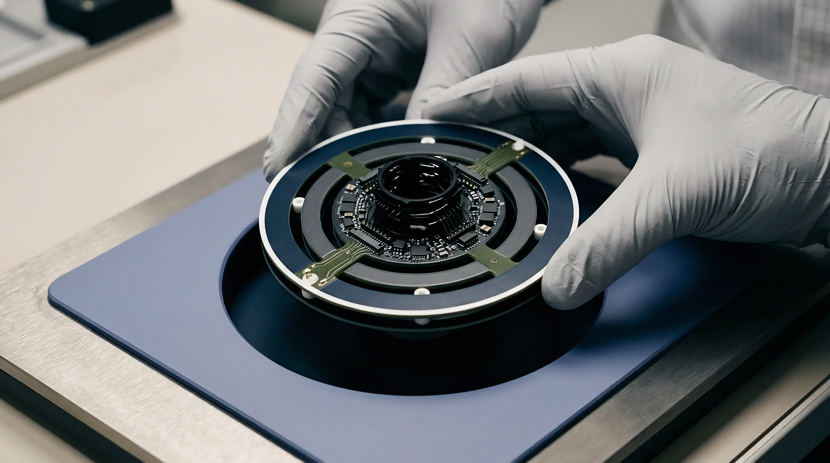
Why Does Thermal Dissipation Accelerate Frequency Chirp during Bursts?
A temperature gradient across the crystal blank changes acoustic velocity unevenly over the vibrating area. When heat enters one edge of the blank, the resulting gradient (Δ T / Δ x) forms across the resonator plane, shifting frequency dynamically.
This temporary temperature gradient alters acoustic wave speed before the crystal can stabilize thermally. As the transmit burst ends, the decaying gradient produces carrier chirp across the frame, moving frequency too quickly for receiver tracking loops to settle.
Physical separation of oscillator components from power amplifier heat sinks prevents rapid dielectric drift during transmit bursts.
Layout isolation strategies help shield sensitive reference resonators from these combined thermal and electrical transients.
| Isolation Technique | Thermal Resistance Increase (K/W) | Transient Voltage Droop (mV) | Frequency Pulling (ppm) | Transmit Pulse EVM Impact |
|---|---|---|---|---|
| Solid copper pour connecting PA ground directly to crystal ground pads | 2.1 | 120 | 18.4 | Degraded by 8.2 dB due to ground bounce and thermal conduction. |
| Thermal relief isolation cuts on internal copper planes around crystal area | 18.5 | 115 | 6.2 | Improved by 4.1 dB through localized thermal attenuation. |
| Dedicated LDO regulator supplying Pierce oscillator rail independently of PA | 18.5 | 12 | 2.1 | Restored to nominal baseline floor (-38 dB EVM). |
| Pi-network attenuation resistor (Rq) limiting crystal peak drive power | 18.5 | 12 | 0.8 | Complete elimination of non-linear DLD frequency offset. |
Cutting thermal relief trenches and adding ground guard traces between RF power transistors and the crystal reduces acoustic frequency drift more effectively than shielding cans alone.

Qualification
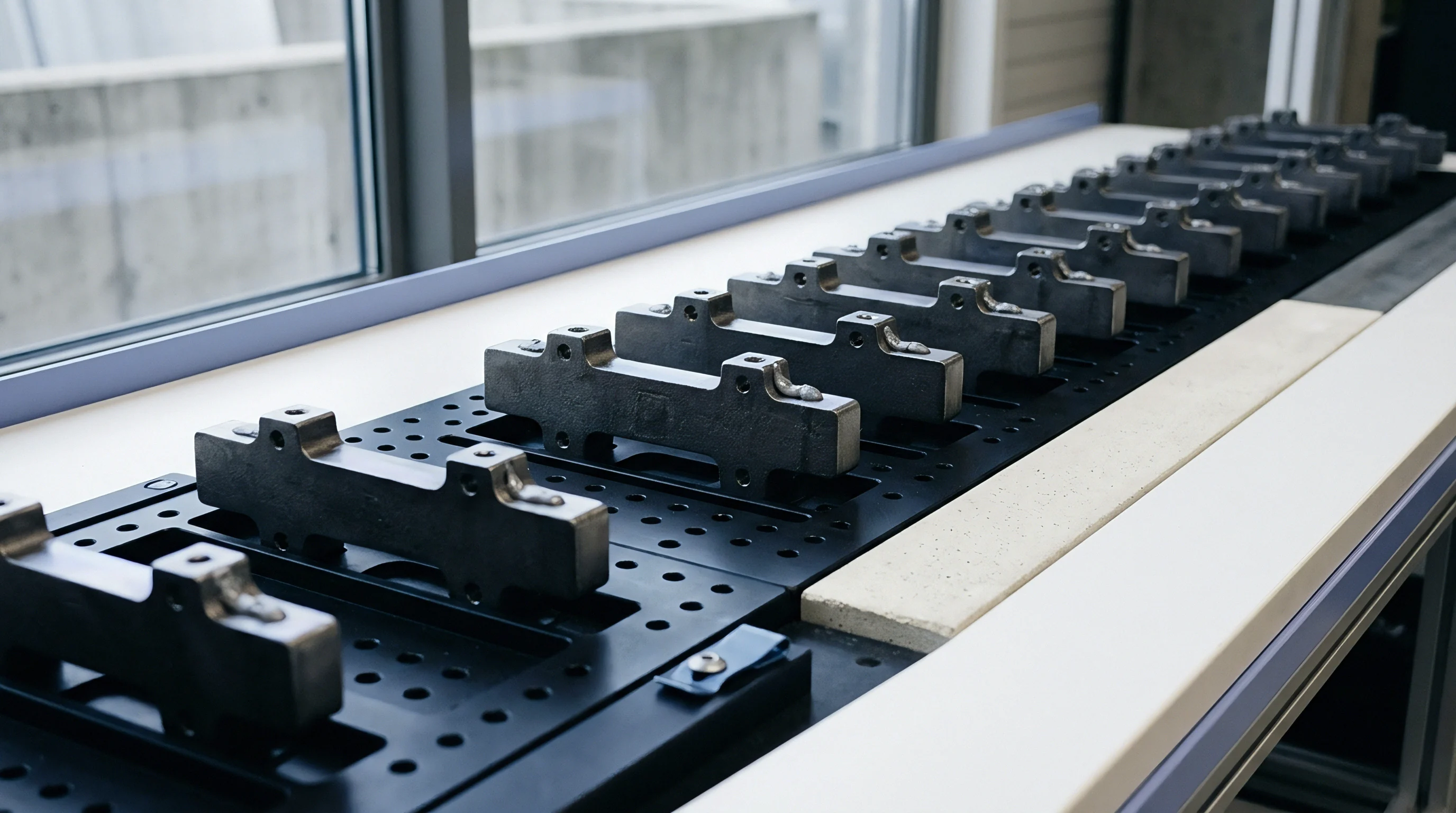
Capturing transient frequency pulling during RF bursts requires fast measurement tools. Standard frequency counters average readings over 100 ms to 1 second gates, hiding millisecond-scale shifts inside a transmit frame. Bench setups must record power supply current, crystal drive voltage, and RF carrier frequency at the same time.
A complete test bench uses a high-bandwidth current probe, an oscilloscope for oscillator voltage, and a real-time spectrum analyzer for time-domain frequency sweeps. Active probes must keep parasitic capacitance under 0.8 pF to avoid loading the crystal circuit, which would distort measured loop gain and drive levels.

Bench Measurement Architecture
A dual-channel real-time spectrum analyzer tied to a near-field magnetic probe monitors carrier shift alongside supply current. Transmit triggering comes directly from a firmware GPIO pin aligned with PA ramp-up, allowing simultaneous logging of supply current and RF phase response in time-aligned buffers.
Drive power calculation requires measuring the peak-to-peak voltage (Vpp) across the crystal terminals during transmit pulses. Drive power (Pd) is calculated using the established formula:
Pd = frac12 · R1 · (2 · π · f0 · CL · Vpp)2
where R1 represents motional resistance, f0 denotes nominal frequency, and CL specifies total load capacitance including PCB parasitic values. Drive level dependency becomes clear when comparing Pd values during idle reception against active high-power transmission phases.
Compliance with AEC-Q200 Grade 2 drive level dependency limits prevents oscillator stall events under dynamic supply voltage ripples.

Step-by-Step Transmit Burst Characterization
Evaluating crystal suitability under dynamic transmit conditions demands a repeatable bench validation sequence.
- Instrumentation Synchronization connects the radio module control interface, digital power supply, current probe, and real-time spectrum analyzer to a common ten megahertz reference clock.
- Quiescent Drive Verification measures crystal voltage amplitude, motional resistance, and operating frequency while the radio operates in continuous receive mode at ambient baseline temperatures.
- Burst Power Triggering configures the device under test to emit maximum output power bursts at defined duty cycles ranging from one percent to fifty percent.
- Time-Domain Frequency Capture logs carrier frequency variation (Δ f) versus time across the entire duration of the transmit pulse, recording initial frequency jump and thermal drift slopes.
- Supply Margin Stressing drops the incoming supply voltage systematically to simulate battery discharge, recording the threshold where motional resistance increase quenches oscillation.
Whether low-power crystal blanks can withstand multi-year cyclic thermal shock from millisecond power amplifier bursts without cumulative lattice degradation remains an open topic for long-term reliability modeling.

Procurement
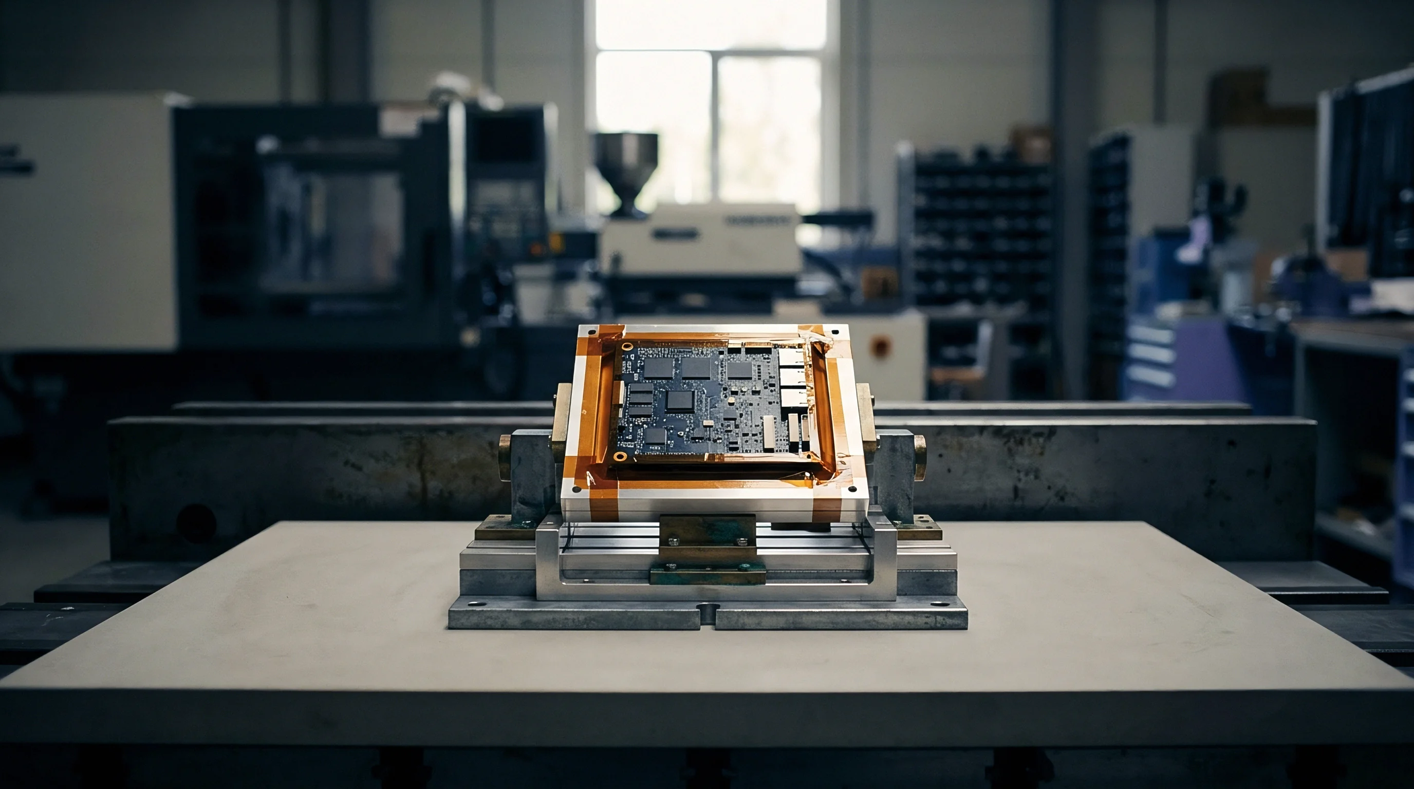
Datasheets rarely capture dynamic drive characteristics, usually specifying maximum equivalent series resistance (R1) at a single power level like 10,μW. That static figure misses the non-linear shifts that happen when transmit current surges push drive levels higher.
Component specifications need explicit DLD limits across the expected power range. Standard commercial specs leave unquantified risks in high-power wireless hardware, making sweep limits on resistance and frequency essential additions to procurement drawings.
Datasheet Parameter Verification
Qualifying crystals for high-power radios requires bounding resistance changes across drive power. Engineering specifications rely on two core parameters here: resistance variation ratio (DLDR1) and frequency shift limit (DLDfreq).
The parameter DLDR1 measures the difference between maximum and minimum motional resistance measured across a drive power sweep from 0.01,μW up to 300,μW:
DLDR1 = R1,max – R1,min
DLDfreq tracks maximum frequency offset over the same sweep. Reliable radio builds enforce tight bounds on both metrics across incoming component lots.
- Drive Level Resistance Delta caps maximum DLDR1 to less than ten ohms across drive power sweeps from sub-microwatt levels to five hundred microwatts.
- Drive Level Frequency Pulling Limit restricts DLDfreq within a tight boundary of plus or minus two parts per million across the full specified operating temperature spectrum.
- Maximum Drive Level Capability guarantees crystal survival and linear operation up to one milliwatt excitation without permanent lattice distortion or parameter degradation.
- Motional Resistance Ceiling specifies an absolute upper boundary for R1 under maximum drive power, ensuring oscillator loop gain margin remains above three across supply droop events.
Contractual Acceptance Thresholds
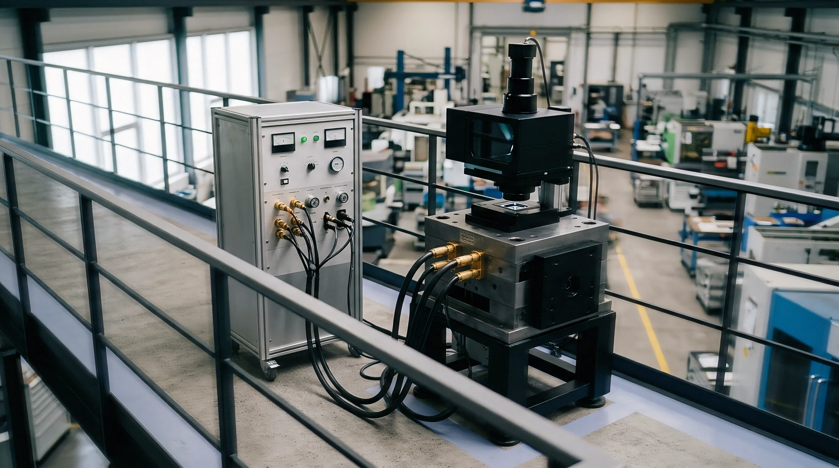
Procurement documents set pass thresholds for drive level stability before volume sign-off. Quality protocols require sweep testing on sample batches following standards like IEC 60444-6.
Supply contracts link lot acceptance directly to dynamic drive performance to manage field risk.
Per IEC standard 60444-6 clause 5.3, crystal lots delivered under purchase agreement 884-B must demonstrate DLDR1 values below eight ohms across a 0.1 to 200 microwatt excitation sweep, where failure to meet this parameter grants the buyer immediate batch rejection rights and mandatory supplier corrective action.