Meaning
A circuit structure creates the necessary electrical bridge between a wireless transceiver output and a radiating component to adjust the load impedance presented to the power source. The antenna matching network handles the transformation of a specific complex impedance to a real value, usually fifty ohms, across a target frequency band. Successful implementation prevents signal reflection back into the amplifier while ensuring maximum power reaches the antenna for efficient propagation.
This interface resides between the filter bank and the actual connector or trace antenna, forming the final boundary of the radio frequency front end. Components within the circuit typically include high frequency inductors and capacitors arranged in shunt or series configurations. Designers use an antenna matching network to account for layout variations and antenna detuning caused by nearby metallic objects or enclosure plastic.
Topology Configuration
Selection of a specific circuit arrangement depends on whether the load impedance sits above or below the characteristic target in the smith chart. A simple L shape circuit uses two reactive elements to move the load to the center point of the graph, while a pi or T structure adds a third element to allow for broader bandwidth or control over the circuit Q factor. Most embedded modules utilize these three element varieties because they offer greater flexibility when adjusting for assembly tolerances or variations in dielectric constants between board batches.
Placing these components close to the feed point reduces trace parasitics that would otherwise introduce unmodelled phase shifts. Standard passive elements must possess high quality factors to avoid heat generation or signal attenuation within the network. Low tolerance components ensure that performance remains consistent over thousands of produced units.
Tuning Procedure
Optimization of values occurs during the hardware verification stage using a calibrated vector network analyzer connected at the feed line breakpoint. Engineers measure the initial return loss to determine the raw impedance of the antenna within its final plastic housing. The values inside the antenna matching network are then calculated based on these measurements using simulation software or smith chart calculations.
Initial prototypes use zero ohm resistors to facilitate simple bypass for these measurements. Once the calculation is complete, specific inductor and capacitor values are soldered into place and verified through a second pass of s parameter testing. This iterative process accounts for the specific parasitics of the copper pads and nearby ground shapes.
Verification Protocol
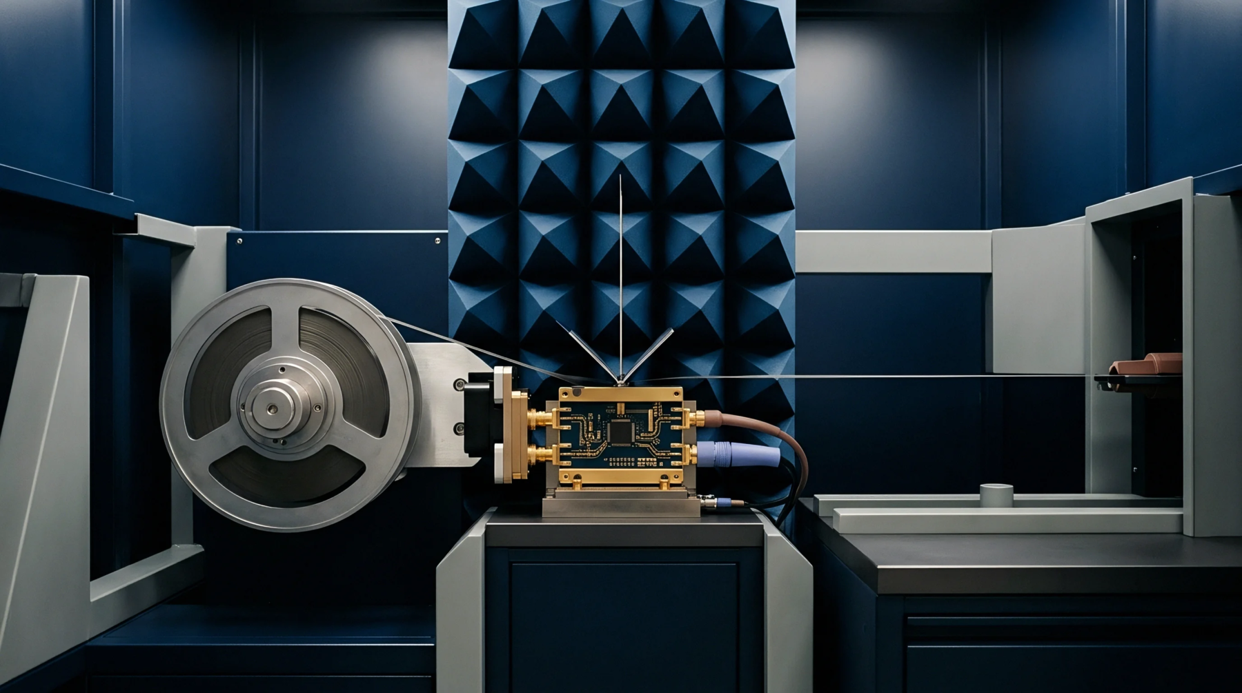
Final qualification requires checking the total radiated power and total isotropic sensitivity of the complete device within an anechoic chamber. An antenna matching network that looks perfect on a cable test may fail in actual operation if the enclosure affects the radiation pattern or near field behavior. Testing must cover the entire range of potential operation channels to ensure the impedance does not drift significantly at the frequency edges.
Environmental stress testing also confirms that physical changes in the circuit board do not shift the center frequency of the matching solution. Large shifts usually indicate excessive parasitic coupling or unstable mounting for the surface mount devices. Data gathered during these chamber tests forms the basis for the final certification submission to regulatory bodies.
Final measurements prove the system complies with maximum power and unwanted emission limits.