Assessing Antenna Detuning Caused by Host Enclosure Modifications
Host enclosure modifications alter near field dielectric loading pulling antenna resonance out of band, degrading radiated efficiency, and forcing regulatory filings.

Dielectric
Near Field Capacitive Loading Mechanics
Positioning a plastic or metallic enclosure shell within the reactive near-field region of an integrated antenna alters the phase velocity and spatial distribution of the electromagnetic wave. The reactive near field extends outward to a boundary distance calculated as the wavelength divided by two times pi, placing the structural wall of most handheld, desktop, and industrial IoT devices well inside the reactive zone at sub-6 GHz operating frequencies. When a plastic housing with a dielectric constant greater than unity enters this space, the effective permittivity surrounding the radiating element increases.
This change elevates the distributed capacitance of the antenna trace relative to its reference ground plane, pulling the natural resonant frequency downward.
The magnitude of this frequency drift depends on the material relative permittivity, the loss tangent, structural thickness, and wall proximity. A standard poly-carbonate housing placed within one millimeter of a 2.4 GHz meandered inverted-F antenna lowers the center frequency by 80 to 140 MHz, shifting the minimum return loss point entirely outside the intended operating band. Introducing structural ribs, snap-fit lattices, or internal BOSS features creates localized variations in the surrounding dielectric field.
These non-uniform boundaries distort the resonant structure unevenly, introducing secondary resonance modes or splitting a single narrow resonance peak into overlapping, degraded response profiles.
| Material Designation | Relative Permittivity | Loss Tangent | Wall Thickness | Spacing to Element | Resonant Shift |
|---|---|---|---|---|---|
| Polycarbonate (PC) | 2.9 | 0.009 | 1.5 mm | 0.8 mm | -110 MHz |
| ABS Plastic | 2.7 | 0.005 | 2.0 mm | 1.0 mm | -85 MHz |
| PC/ABS Alloy | 2.8 | 0.007 | 1.8 mm | 0.5 mm | -135 MHz |
| Polyamide (Nylon 6,6) | 3.6 | 0.021 | 1.5 mm | 0.8 mm | -165 MHz |
| Anodized Aluminum Shell | Metallic Boundary | Infinite | 1.2 mm | 3.0 mm | -210 MHz |

Conductive Proximity and Eddy Current Damping
Metallic components within the host housing introduce different operational failures. Internal battery packs, printed circuit board shield cans, flexible printed circuit cables, and decorative metallized overlays act as conductive boundaries that image the antenna current. Bringing a conductive sheet within the near field creates counter-circulating eddy currents that oppose the primary radiating current vector.
This interaction reduces the radiation resistance of the element, driving the real part of the input impedance down from fifty ohms toward single-digit values while introducing strong inductive or capacitive reactance depending on the current distribution on the metal structure.
Paint coatings containing metallic flakes or electromagnetic interference shielding sprays inside the plastic casing generate similar shorting conditions. High-surface-resistivity coatings reduce the antenna total radiation efficiency by absorbing electromagnetic energy as heat within the resistive film rather than allowing it to radiate into free space. Absorptive loss directly depresses the total radiated power without altering the voltage standing wave ratio in a way that alerts the engineer on a simple scalar reflection measurement.
Relative permittivity increases in the reactive near field force the antenna electrical length outward, pulling the primary resonance below the targeted passband.
Host Modifications and Coupling Pathways
- Structural Wall Thickening increases total capacitive loading, driving the fundamental resonance frequency downward while decreasing the operational bandwidth across the operating channel allocation.
- Internal Metallic Shielding Spray converts near-field reactive energy into surface thermal dissipation, sharply lowering total radiation efficiency while shifting input impedance toward a low resistive value.
- Battery Pack Relocation introduces a massive virtual ground plane that distorts the current paths across the motherboard layout, generating asymmetric radiation nulls in the far-field pattern.
- Potting Compound Encapsulation replaces the air boundary with a dense dielectric medium, altering the velocity factor of the antenna conductors and displacing the resonant center frequency by hundreds of megahertz.
Modifying a plastic enclosure by adding internal stiffening ribs or changing resin formulations alters the environmental boundaries of the radio module. Selecting high-loss resins like wet polyamide introduces temperature-dependent and moisture-dependent detuning behavior during operation. A housing that passes bench validation in a dry environment shifts out of band when relative humidity causes water absorption within the nylon material matrix.
Neglecting the thermal and dielectric variance of structural plastics leads to field failures where transmitter output power drops below receiver sensitivity thresholds across operational temperature extremes.

Impedance

Vector Network Analyzer Measurement Execution
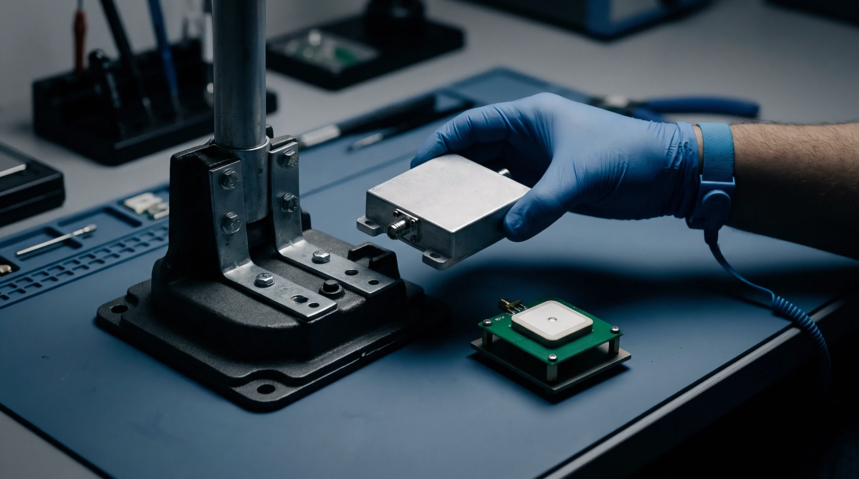
Quantifying the precise detuning caused by enclosure modifications begins with accurate reflection measurements taken directly at the antenna feed port. Connecting a calibrated Vector Network Analyzer (VNA) requires a micro-coaxial pigtail soldered to the feed trace, keeping ground connections under two millimeters in length to minimize parasitic lead inductance. The operator executes a full one-port vector calibration at the cable end-point using Open-Short-Load standards to displace the measurement reference plane directly to the input terminals of the matching network.
Measuring the bare circuit board in free space establishes the baseline primary reflection coefficient curve, recorded as S11 across the designated frequency band. The engineer then places the PCB assembly into the original unmodified enclosure and subsequently into the modified host housing, sweeping the band from 1.0 GHz to 6.0 GHz to record S11 phase and magnitude. Comparing these curves on a Smith Chart reveals both the resistive real shift and reactive imaginary movement caused by the housing geometry changes.
Quantifying S11 and VSWR Degradation
A properly tuned antenna exhibits an S11 return loss better than negative ten decibels, corresponding to a Voltage Standing Wave Ratio (VSWR) below 2.0:1 across the operating band. When host enclosure modifications bring dielectric material closer to the radiator, the S11 dip shifts down in frequency, degrading the return loss at the intended operational carrier frequency. A shift that moves the S11 dip from 2.45 GHz down to 2.32 GHz can raise the return loss at 2.45 GHz from negative fifteen decibels to negative two decibels.
A return loss of negative two decibels means that approximately sixty percent of the RF power delivered by the power amplifier bounces back from the antenna port toward the transmitter. This reflected power generates thermal stress in the front-end module, accelerates power amplifier gain compression, and reduces the power actually launched into the air. The table below illustrates the relationship between S11 return loss, VSWR, reflected power percentage, and mismatch loss incurred at the antenna terminal.
| Return Loss S11 (dB) | VSWR (:1) | Reflected Power (%) | Transmitted Power (%) | Mismatch Loss (dB) |
|---|---|---|---|---|
| -20.0 | 1.22 | 1.00 | 99.00 | 0.04 |
| -15.0 | 1.43 | 3.16 | 96.84 | 0.14 |
| -10.0 | 1.92 | 10.00 | 90.00 | 0.46 |
| -6.0 | 3.01 | 25.12 | 74.88 | 1.26 |
| -3.0 | 5.85 | 50.12 | 49.88 | 3.02 |
| -1.0 | 17.39 | 79.43 | 20.57 | 6.87 |
Evaluating Complex Impedance Trajectories on the Smith Chart
Reading the reflection trajectory on the Smith Chart clarifies the physical nature of the enclosure interaction. Pure dielectric loading moves the resonance loop clockwise along lines of constant conductance while expanding the loop radius due to added dielectric loss. Conductive proximity reduces the resistance circle size, forcing the locus toward the short-circuit point at the far left edge of the chart.
Tracking the locus movement provides the exact series inductance, series capacitance, parallel inductance, or parallel capacitance required to pull the complex impedance back to the central fifty-ohm origin point. If the modification introduces strong reactive reactance, the impedance point leaves the stable matching zone entirely, rendering simple two-element matching topologies inadequate for wideband operation.
An S11 return loss degradation from fifteen decibels to three decibels causes half of the transmitted radio frequency energy to reflect directly back into the output stage.
Suppliers frequently defend baseline antenna performance figures by stating that the reference circuit board was verified in free space using ideal ground planes. This defense ignores the structural reality that no commercial radio operates suspended in free space without a housing. When an integrated product exhibits dropped connections or elevated thermal dissipation in the field, relying on vendor-supplied free-space S-parameter files shifts the failure directly onto the host integration process.


Pattern

Anechoic Chamber 3d Spatial Radiation Characterization
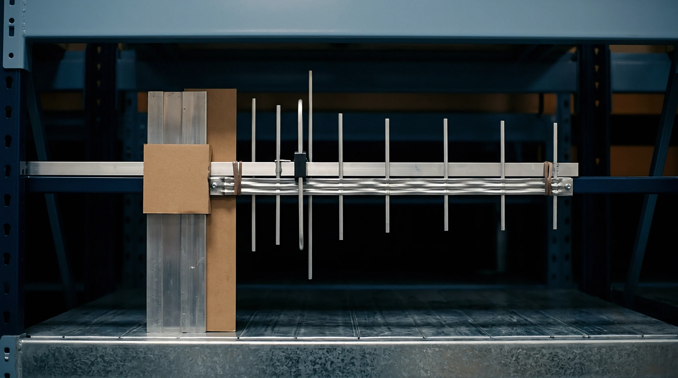
Assessing total radiated performance requires placing the complete host assembly inside a fully anechoic test chamber equipped with a multi-axis positioner and calibrated dual-polarized measurement horns. The test system rotates the host housing through 360 degrees of azimuth and 180 degrees of elevation, sampling the radiated electric field strength at precise angular increments across the three-dimensional sphere. These spherical field samples generate full spatial radiation patterns, allowing calculation of Total Radiated Power (TRP) and Total Isotropic Sensitivity (TIS).
Modifications to the host enclosure disrupt the spatial distribution of energy even when the matching network is adjusted to restore a negative ten decibel S11 return loss. Metallic structural brackets, internal wiring harness rerouting, or structural enclosure cutouts alter the surface currents flowing along the host PCB ground plane. These altered surface currents reshape the far-field pattern, turning an omnidirectional radiation pattern into an asymmetric distribution characterized by deep spatial nulls.
| Enclosure Offset Distance | Peak EIRP (dBm) | TRP (dBm) | TIS (dBm) | Max Pattern Null Depth (dB) |
|---|---|---|---|---|
| Free Space (No Shell) | +18.5 | +16.2 | -92.1 | -4.2 |
| 5.0 mm Clear Plastic | +18.1 | +15.8 | -91.5 | -5.1 |
| 2.0 mm Clear Plastic | +16.8 | +14.3 | -89.2 | -9.8 |
| 1.0 mm Clear Plastic | +14.2 | +12.1 | -86.0 | -15.4 |
| 1.0 mm Plastic + Shield Paint | +8.5 | +5.1 | -78.2 | -24.6 |
Depression of Total Radiated Power and Isotropic Sensitivity
Total Radiated Power measures the integral of all RF energy launched into space over the entire spherical boundary. A material change that increases dielectric absorption losses directly lowers the TRP value. If an unmodified enclosure yields a TRP of plus sixteen decibels milliwatts and a modified housing with carbon-black pigment reduces TRP to plus twelve decibels milliwatts, the product loses four decibels of effective link margin in every direction regardless of receiver orientation.
Total Isotropic Sensitivity characterizes the spatial receiver performance by integrating effective sensitivity across the sphere under real operating conditions. TIS degradation occurs rapidly when host enclosure modifications couple digital noise sources closer to the antenna element. A shifted enclosure wall that forces a display flex cable closer to the antenna structure allows high-harmonic processor noise to enter the receiver front end, degrading TIS from negative ninety-two decibels milliwatts to negative eighty-two decibels milliwatts.
This ten-decibel reduction in sensitivity cuts the operational communication range of the device in half.
Spurious Emissions Dynamics under Detuned Conditions
Detuning an antenna alters the harmonic load impedance seen by the power amplifier output stage. Transmit power amplifiers are designed to drive a nominal fifty-ohm load; presenting a detuned, reactive load causes non-linear operation and raises the level of second and third harmonic emissions generated within the silicon die. The antenna structure, now detuned at the fundamental operating frequency, may unexpectedly present higher radiation efficiency at these harmonic frequencies.
A product that comfortably passed radiated spurious emissions limits in its preliminary evaluation can fail regulatory limits at the second harmonic frequency following an enclosure modification. The elevated harmonic output combines with altered radiation directivity, creating localized field strengths that exceed peak limits specified under regional standards. Detecting these emissions requires sweeping the anechoic chamber up to the tenth harmonic frequency with the product operating at maximum rated output power.
Harmonic load pull caused by fundamental antenna detuning increases transmitter non-linear distortion, raising radiated second-harmonic emissions above regulatory thresholds.
What degree of spatial radiation pattern distortion remains acceptable before a host device loses operational certification under carrier-specific over-the-air requirements?
Scope

Federal Communications Commission Permissive Change Framework
Modifying a host enclosure that houses a certified modular transmitter requires evaluating the regulatory status under FCC guidance documents, specifically KDB 996369 D02 and D04. The FCC modular approval framework distinguishes between changes that maintain identical RF characteristics and those that alter radiated field intensity or spurious emission profiles. If the host modification causes antenna detuning that alters the fundamental radiated power or changes the physical distance between the antenna and external structural walls, the host integrator must classify the change under official filing categories.
A Class I Permissive Change (C1PC) applies when enclosure modifications do not increase radiated emissions or change the RF parameters authorized under the original grant. If the detuning degrades antenna gain or shifts resonant frequencies such that re-tuning via matching components is needed, but the final radiated field strength remains lower than or equal to the original certified levels, a C1PC is filed via internal documentation. If the modification causes an increase in any radiated harmonic or spurious emission, or if a different antenna type or higher gain configuration is introduced, a Class II Permissive Change (C2PC) is required, involving official laboratory test report submissions to a Telecommunications Certification Body (TCB).
European Union Radio Equipment Directive Re-Assessment Mandates
Under the European Union Radio Equipment Directive (RED) 2014/53/EU, host integrators cannot rely on a supplier modular grant without taking full legal responsibility for final product conformity. Article 3.2 of the Directive demands that radio equipment effectively use the radio spectrum and support the efficient use of spectrum to avoid harmful interference. When a host enclosure modification causes antenna detuning, the integrated product must be re-evaluated against applicable Harmonised Standards, such as ETSI EN 300 328 for 2.4 GHz wideband systems or ETSI EN 300 220 for sub-1 GHz devices.
Re-assessment requires verifying effective isotropically radiated power (EIRP), maximum power spectral density, occupied channel bandwidth, and transmitter transmitter unwanted emissions in the out-of-band and spurious domains. If dielectric loading from the modified housing shifts the antenna resonance and causes out-of-band emissions to spill across channel boundaries defined in ETSI EN 300 328 clause 4.3.2.8, the manufacturer cannot sign the EU Declaration of Conformity. The host manufacturer must perform physical re-testing in an accredited facility and place the updated test reports into the technical construction file prior to placing the product on the market.
- Evaluate Host Change Delta where mechanical engineers document every material, thickness, and spacing modification applied to the enclosure assembly.
- Conduct Bench Pre-Scan Verification using a calibrated VNA to measure S11 return loss and verify if the fundamental resonance remains within the target frequency mask.
- Perform Radiated Spurious Emissions Sweep in a semi-anechoic chamber up to 40 GHz under ANSI C63.10-2013 test procedures to detect non-linear harmonic amplification.
- Determine Certification Route Classification by comparing measured radiated data against original grant parameters to choose between C1PC, C2PC, or full new Equipment Authorization.
- Update Technical Construction File with signed laboratory reports, modified assembly drawings, and updated matching network schematics for market surveillance audits.
Which Host Changes Trigger a Permissive Filing?
Determining whether a host enclosure alteration forces a formal regulatory permissive change filing depends on specific physical threshold metrics. Changing the material composition of the housing from a non-conductive resin to a conductive or carbon-filled polymer alters the original certification conditions entirely. Reducing the physical spacing between an integrated trace antenna and the outer skin of the host housing by more than twenty percent invalidates the SAR exclusion distances established in the original modular grant.
Adding internal metallic structural stiffeners, thermal heat sinks, or ground grounding clips within the reactive near field of the antenna alters the antenna radiation pattern and efficiency. When these physical changes cause radiated spurious field strength to increase by more than three decibels over the original module test report values, even if still below the absolute regulatory limit, the change triggers a Class II Permissive Change filing under FCC rules. The table below outlines structural modification conditions and their corresponding regulatory filing obligations across key global jurisdictions.
| Physical Enclosure Modification | FCC Market Status (USA) | EU RED Status (Europe) | ISED Status (Canada) |
|---|---|---|---|
| Plastic resin change (Identical Er) | Class I Permissive Change | Internal TCF Documentation | Class 1 Permissive Change |
| Plastic resin change (Er increase > 0.5) | Class II Permissive Change | Article 3.2 Retests Required | Class 2 Permissive Change |
| Addition of internal metallic shield | Class II Permissive Change | Full Radiated Retest | Class 2 Permissive Change |
| Antenna-to-wall distance reduced > 20% | Class II Permissive Change + SAR | Article 3.1(a) SAR Re-assessment | Class 2 Permissive Change + SAR |
| Conductive paint application | Class II Permissive Change | Full Radiated Retest | Class 2 Permissive Change |
Harmonised standard ETSI EN 300 328 clause 4.3.2.8 obligates host manufacturers to prove that transmitter out-of-band domain emissions remain fully contained within allocated band edges under final enclosure assembly conditions.
Ignoring permissive change classification rules risks product impoundment at regional entry customs and invalidates commercial product insurance policies.

Topology
Pi-Network Matching Architecture and Component Selection
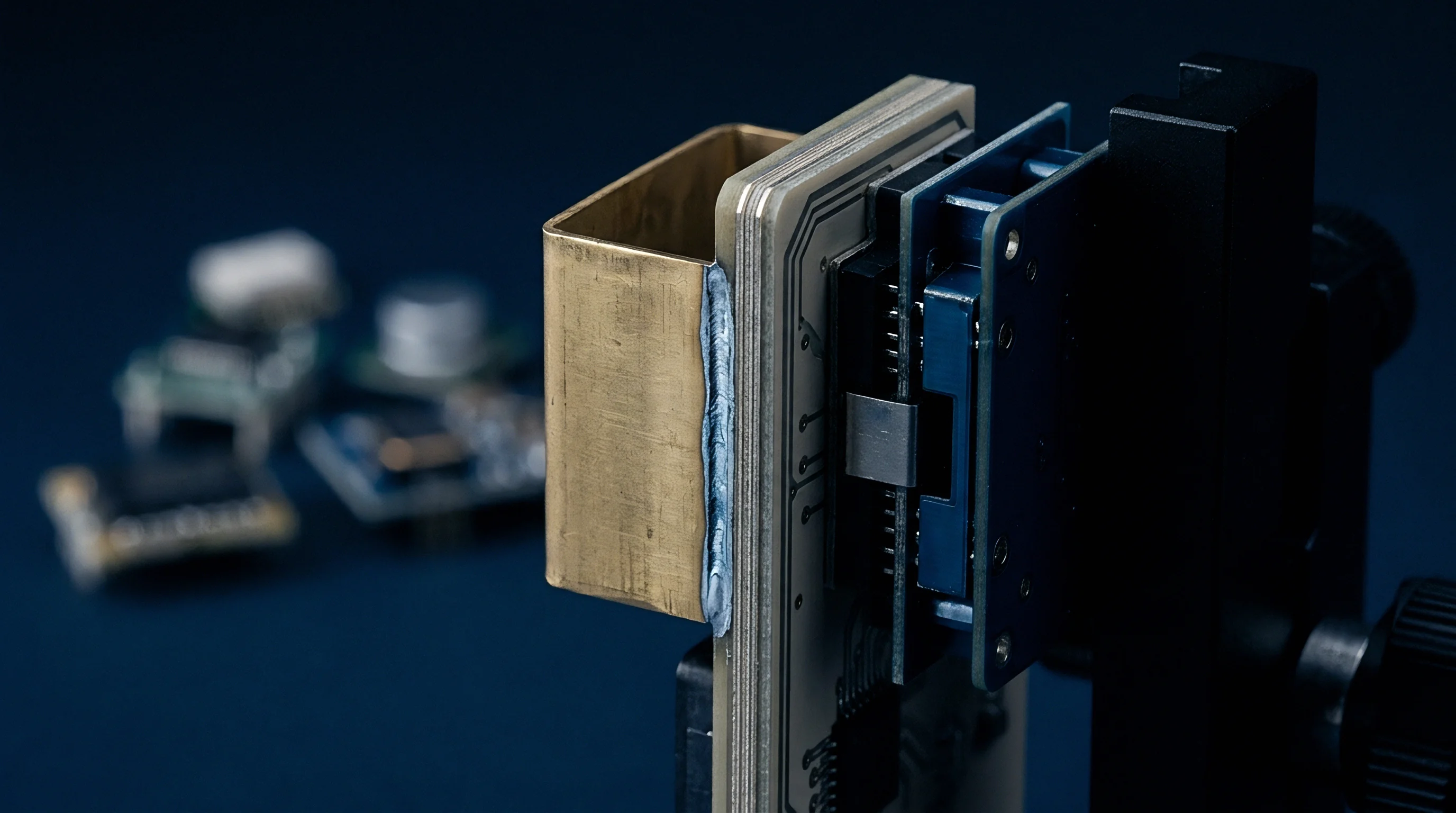
Remediating the detuning effects caused by host enclosure modifications requires implementing a flexible matching network directly between the radio module output pin and the antenna feed structure. The standard hardware topology consists of a three-element Pi-network, configured with one series component slot and two parallel component slots to ground. This arrangement provides full two-dimensional coverage on the Smith Chart, allowing the engineer to transform complex detuned impedances back to the target fifty-ohm real impedance axis.
Selecting components for the Pi-network requires careful consideration of parasitic elements and component quality factors (Q-factor). High-Q RF inductors with self-resonant frequencies well above the operational band avoid unwanted internal series resonances. Capacitors must feature tight tolerances, typically plus or minus 0.1 picofarads for low values, constructed from C0G/NP0 dielectric materials to prevent capacitance drift over temperature extremes.
Using low-grade commercial chip inductors with high DC resistance introduces insertion loss, converting precious transmitter RF power into heat before it reaches the antenna element.

Vector Smith Chart Transformation Procedure
Tuning the network involves a systematic progression on the calibrated VNA Smith Chart display. The engineer first measures the raw, un-matched antenna impedance inside the fully assembled, modified host housing. This un-matched point establishes the starting impedance z-zero.
The goal is to move z-zero along constant resistance and constant conductance circles until it lands precisely at the center point where impedance equals fifty plus j-zero ohms.
If the un-matched impedance sits in the lower inductive half of the chart due to near-field capacitive loading from the plastic housing, the engineer adds a series inductor to rotate the locus clockwise along a constant resistance circle. If the resistive component has dropped below fifty ohms, a parallel inductor or parallel capacitor is added first to move the point along a constant conductance circle to the intersect line. Iteratively swapping surface-mount component values transforms the shifted impedance, restoring the S11 curve to a deep notch centered on the operational frequency band.

Matching Component Selection Parameters
- Inductor Quality Factor must exceed thirty at the operating frequency to prevent resistive insertion losses from degrading system efficiency.
- Self-Resonant Frequency Margin demands choosing components whose internal resonance sits at least two times higher than the operating carrier.
- Dielectric Thermal Stability requires specifying C0G/NP0 ceramic capacitors to prevent temperature variation from detuning the matching network.
- Package Parasitic Reactance mandates using small 0201 or 0402 surface-mount component footprints to minimize trace pad parasitic capacitance to ground.
Positioning matching components further than three millimeters away from the antenna feed pad introduces transmission line phase rotation that complicates the network transformation topology.


Ledger

Chamber Time, Sample Logistics, and Retest Financials
Correcting for antenna detuning late in the product development cycle generates measurable direct fees and schedule slip. Booking time in an accredited fully or semi-anechoic testing chamber costs between 250 and 450 US dollars per hour, with full-day blocks running up to 3,500 US dollars per shift. Quantifying the total impact requires factoring in engineering setup time, VNA matching sessions, over-the-air TRP/TIS measurements, and radiated emissions testing across all required operating channels.
Sample preparation introduces additional expense. Regulatory bodies and test laboratories require multiple identical host units configured in specific operational test modes. Obtaining, assembling, and modifying four to six fully operational host prototypes with special test firmware and RF pigtail breakouts adds thousands of dollars in prototype material and labor expenses.
If initial pre-scans reveal radiated spurious emission failures due to detuning, the testing campaign stops, forfeiting the booked chamber slot fee while mechanical redesign takes place.
| Regime / Filing Class | Laboratory Chamber Hours | Filing / TCB Fees (USD) | Sample Count Required | Schedule Lead Time Impact |
|---|---|---|---|---|
| FCC Class I Permissive Change | 4 – 8 Hours | $0 (Internal File) | 1 Unit | 1 – 2 Weeks |
| FCC Class II Permissive Change | 12 – 24 Hours | $3,500 – $5,500 | 2 – 3 Units | 4 – 6 Weeks |
| EU RED Article 3.2 Re-test | 16 – 32 Hours | $4,000 – $8,000 | 2 – 4 Units | 3 – 5 Weeks |
| ISED Canada Class 2 Change | 12 – 20 Hours | $2,500 – $4,000 | 2 Units | 4 – 6 Weeks |
| Full Global Re-Certification | 60 – 100 Hours | $25,000 – $45,000 | 6 – 10 Units | 10 – 14 Weeks |

Schedule Slippage and Commercial Market Entry Penalty
The time required to resolve an antenna detuning failure stretches product release timelines significantly. Securing an emergency chamber booking slot at a primary accredited test house typically involves a two-to-four-week queue delay. Executing the physical testing, analyzing the resulting data, and generating a formal accredited test report takes another two weeks.
Submitting the paperwork to a TCB for an FCC Class II Permissive Change grant adds three to fifteen business days depending on TCB workload and administrative review cycles.
A six-to-eight-week delay in commercial launch date carries immediate market financial penalties. For consumer electronics tied to holiday shipping windows or industrial deployments governed by strict contractual delivery deadlines, missing the launch date risks order cancellations and distributor inventory penalties. The total financial penalty of an unexpected detuning issue is dominated by lost sales volume and missed market entry windows rather than the direct lab test fees.
Executing an antenna pre-evaluation phase using early structural prototypes inside a 3D-printed host casing limits financial exposure. Validating S11 performance prior to cutting final hard tooling for injection molding ensures that dielectric offsets are integrated into the antenna geometry early, keeping market entry dates intact.