Electromagnetic Coupling Mechanisms Affecting Unintentional Radiated Emissions inside Compact Multi Transmitter Host Enclosures
Internal RF coupling converts near-field reactive energy into unintended far-field emissions through enclosure seams, ground breaks, and unshielded host wiring.

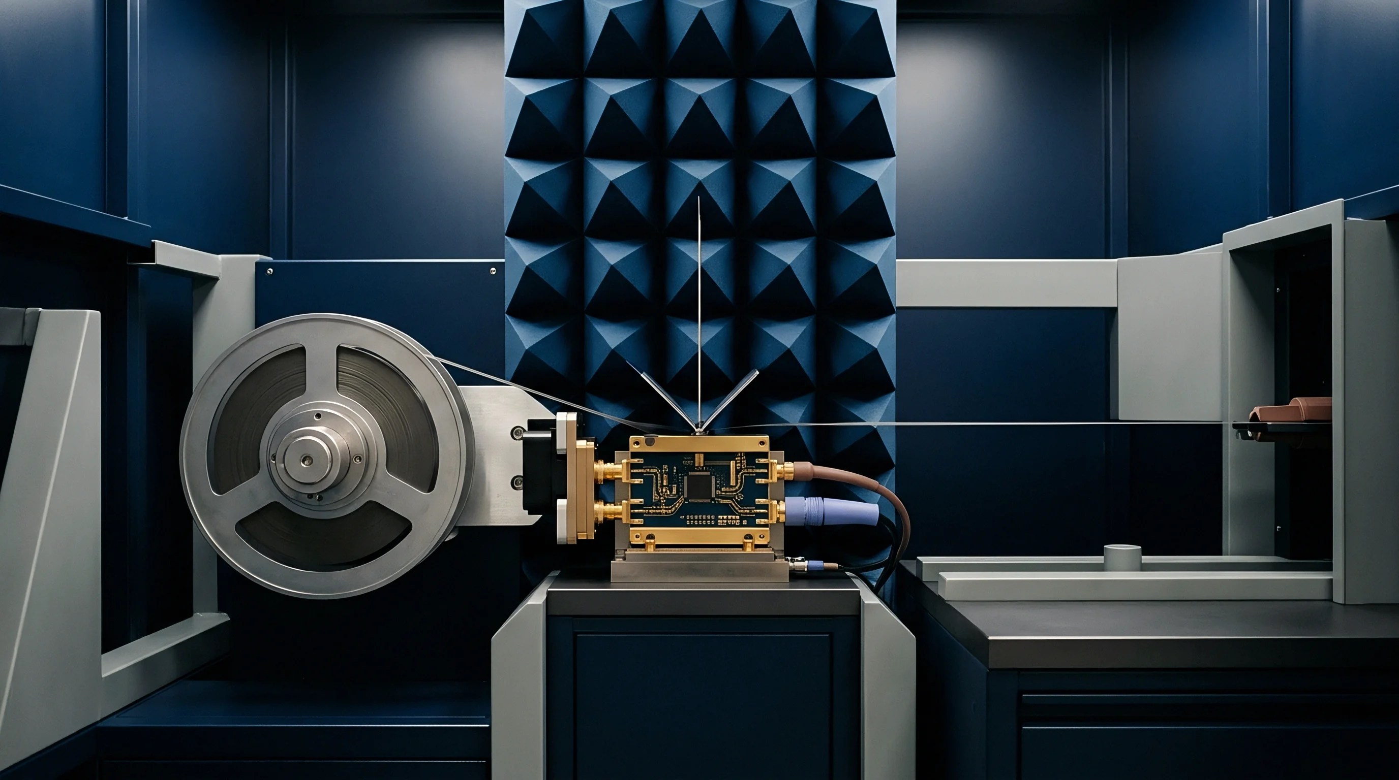
Topology
Packing dense cellular, Wi-Fi, and Bluetooth modules into metallic or metallized plastic housings creates complex reactive field environments. High-density layouts place transmit antennas, power management ICs, digital signal processors, and high-speed data buses within millimeters of each other. At these distances, energy transfers through near-field reactive coupling well before electromagnetic waves propagate into the far field.
The physical arrangement of host boards, component heights, and housing walls dictates whether parasitic energy stays trapped on local traces or converts into unintentional radiated emissions that breach regulatory limits.
Electric field, or capacitive, coupling stems from voltage gradients between adjacent conductive structures. Inside a compact enclosure, high-frequency voltage switching on a microstrip trace or component pin generates a localized electric field that terminates on nearby conductive elements ~ such as adjacent signal traces, ungrounded metallic brackets, or internal shield covers. Coupled voltage magnitude depends on mutual capacitance and the voltage slew rate.
When an internal trace carries high-speed digital data or clock harmonics with sub-nanosecond rise times, capacitive current injected into neighboring paths creates secondary RF sources capable of driving host wiring and chassis seams.
Inductive magnetic field coupling occurs when high-frequency loop currents generate time-varying magnetic flux lines encircling adjacent conductive loops. Multi-transmitter architectures contain numerous signal return loops, power supply decoupling loops, and RF output matching networks. When an active transmitter drives RF power into an antenna feedline, the surrounding magnetic field induces noise voltages in any nearby closed-loop circuit.
Parasitic inductive transfer scales with mutual inductance, loop surface area, and signal frequency. Small loop areas on printed circuit boards reduce magnetic coupling, but tight layout constraints in compact enclosures often force return paths around component keep-out zones, expanding magnetic loops that radiate efficiently inside the housing.
Cavity modes develop inside metallic housings when internal dimensions match integer multiples of half the operational wavelength. Standard multi-radio host housings measuring 80 millimeters by 50 millimeters by 10 millimeters exhibit natural cavity resonances starting near 2.4 GHz. Fundamental emissions or high-order harmonics matching these internal resonant frequencies excite standing electromagnetic waves within the metal enclosure, elevating local field intensities by 15 dB to 20 dB over free-space levels.
This field amplification forces energy through tiny structural seams, display apertures, and connector cutouts, turning internal cavity modes into primary sources of unintentional radiated emissions in semi-anechoic chambers.
Crosstalk between co-located transceivers creates severe operational and compliance risks. Modern host devices regularly integrate 5G sub-6 GHz cellular modems, dual-band or tri-band Wi-Fi 6E/7 modules, and Bluetooth transceivers in a single volume. When a Wi-Fi module transmits at 2400 MHz to 2484 MHz, its near-field RF energy couples directly into printed circuit board traces supplying an adjacent 5G NR module in Band n78 (3300 MHz to 3800 MHz).
This coupling introduces broadband noise, drives non-linear mixing in cellular front-end filters, and induces spurious currents on common ground planes. Mapping these coupling paths across dense board layouts quantifies how parasitic energy transfers between transceivers prior to chassis assembly.
Ungrounded internal shield cans transform localized magnetic fields into electric field radiators across host enclosures.
Near-field reactive coupling usually drives the initial emissions seen during early pre-scans.

Near Field Inductive Coupling Mechanics
Low-frequency magnetic fields generated by PCB loop currents easily bypass thin surface coatings. Magnetic fields pass through non-magnetic metallic foils and thin plating with little attenuation because skin depth at lower RF frequencies exceeds the material thickness. Mutual inductance between a transmitter power amplifier output trace and a nearby board-to-board ribbon cable line dictates the magnitude of induced noise voltage on that cable ~ calculated as mutual inductance multiplied by the rate of change of transmit current over time.
High transmit power combined with rapid RF carrier oscillations drives peak noise voltages onto host wiring.
Cutting mutual inductance requires minimizing loop areas for both the source trace and victim circuit. Placing a solid copper ground reference plane directly beneath RF microstrip traces confines magnetic flux lines to the thin dielectric layer between trace and ground plane, reducing the effective loop area to the substrate’s cross-sectional height. Routing traces across split ground planes or cutouts forces return currents around the gap, expanding the loop area by orders of magnitude.
These expanded loops generate wideband magnetic fields that flood the enclosure cavity and couple into every conductive element inside the housing.

Cavity Modes inside Metallized Housings
An enclosure measuring 60 millimeters by 40 millimeters resonates at fundamental frequencies near 2.5 GHz. Calculating resonant frequencies for rectangular enclosure cavities requires determining mode distribution numbers for transverse electric and transverse magnetic wave patterns. While resonant frequency in a hollow metallic cavity depends on housing wall dimensions and internal dielectric permittivity, real host enclosures contain plastic supports, battery casings, and multi-layer circuit boards.
These materials increase effective permittivity, pulling enclosure mode resonances down to lower frequencies.
Resonance degrades circuit isolation dramatically. At cavity resonance, transfer impedance between an internal RF source and an enclosure aperture reaches peak levels. Small parasitic emissions from digital lines or transceiver harmonics that would otherwise stay harmless are amplified by the cavity’s quality factor.
High Q factors store RF energy efficiently, creating field hot spots near chassis seams and flex cable cutouts. Suppressing these modes requires adding lossy magnetic absorbers or conductive posts that break large cavity volumes into smaller, non-resonant sub-cavities.

Which Aperture Geometry Minimizes Radiation?
Narrow slots perpendicular to surface current vectors leak far more electromagnetic energy than circular arrays. When internal cavity fields strike conductive chassis walls, they induce high-frequency surface currents on interior metal faces that flow toward ground connections and seams. If an aperture interrupts this current path, current must travel around the gap, creating a potential difference across slot edges.
This voltage drop converts the aperture into a slot antenna radiating RF energy directly outside.
Aperture length dictates radiation efficiency. A slot radiates efficiently when its longest dimension reaches half the operational RF wavelength. Multiple small circular ventilation holes with diameters well below half a wavelength attenuate radiated fields effectively through waveguide-below-cutoff action.
By contrast, long, narrow slots formed by mating plastic-to-metal snaps force surface currents to diverge, radiating fields that easily breach international spurious emission limits. Controlling slot radiation requires conductive grounding gaskets, spring fingers, or overlapping tongue-and-groove joints along every structural seam.
| Coupling Mechanism | Dominant Field Type | Primary Physical Driver | Coupling Scaling Parameter | Primary Radiation Path |
|---|---|---|---|---|
| Capacitive (Electric) | High-impedance Electric (E) | Trace-to-trace voltage gradients, dV/dt | Mutual capacitance (C_m) | Chassis cutouts, display flex cables |
| Inductive (Magnetic) | Low-impedance Magnetic (H) | Ground return current loops, dI/dt | Mutual inductance (L_m) | External I/O wiring, unshielded seams |
| Cavity Resonance | Electromagnetic Wave (E & H) | Enclosure dimensions relative to wavelength | Quality factor (Q) of housing cavity | Chassis parting lines, seams, slots |
| Common-Mode Current | Conducted-to-Radiated Conversion | Ground potential differentials across PCB | Transfer impedance (Z_T) | Attached peripheral cables, antenna outer shields |
Unintentional radiated emissions from internal topology interactions create severe certification bottlenecks. When multiple transmitters operate concurrently inside a confined host, measuring near-field coupling strength reveals whether shielding is actually adequate. Chamber scans frequently show unexpected emission peaks caused by subtle interactions between board traces and metal chassis frames.
What specific physical layout changes inside a multi-transmitter housing definitively isolate inductive ground loops without forcing a complete board spin?


Leakage
Physical apertures, enclosure seams, display cutouts, and connector interfaces serve as primary escape paths for trapped RF energy. Metallic host enclosures are rarely single continuous shells; they assemble from cast covers, extruded frames, plastic antenna windows, and stamped internal shields. Every mechanical junction introduces seam impedance where high-frequency surface currents encounter resistance and inductance.
When surface currents cannot flow smoothly across chassis joints, voltage drops develop across seam gaps, driving electromagnetic fields through structural openings and converting internal noise into far-field radiated emissions.
Bethe hole coupling theory establishes how electromagnetic fields penetrate small apertures. When an aperture’s maximum dimension is small compared to the incident wavelength, the slot’s magnetic dipole moment dominates far-field radiation. Radiated power scales with the sixth power of aperture dimension for circular holes, whereas elongated slots scale primarily with the square of their length.
A 15-millimeter slot along a seam radiates significantly more energy at 2.4 GHz than a grid of twenty 1.5-millimeter circular ventilation holes with identical total surface area. Managing chassis radiation means controlling slot lengths rather than total open area.
Surface transfer impedance measures the shielding efficiency of mechanical joints and cable braid terminations. Defined as the ratio of longitudinal electric field generated on a shield or seam’s outer surface to high-frequency current flowing along its inner surface, transfer impedance must stay near zero milliohms per meter to prevent field leakage. Elevated transfer impedance at chassis seams lets internal magnetic fields induce external surface currents that travel along outer metal surfaces, turning the entire chassis into a dipole or patch radiator across spurious bands.
Display interface apertures represent particularly challenging chassis escape paths in compact designs. High-speed protocols like MIPI Display Serial Interface (DSI) or embedded DisplayPort (eDP) route multi-gigabit data across flexible printed circuits (FPCs) bridging motherboard and display panel. These flex circuits run right alongside housing seams and display perimeter gaps.
Transmit power from nearby cellular or Wi-Fi antennas couples into unshielded flex trace loops, inducing common-mode currents. The unshielded flex line then acts as a driving element, coupling RF energy into the metallic display frame and radiating directly out of the front perimeter gap.
Cable shield terminations introduce common-mode noise onto external interconnect cables. When a peripheral cable plugs into a host, its shield must bond cleanly to the metallic chassis or primary PCB ground plane with 360-degree circumferential contact. In ultra-compact designs, space constraints often force engineers to use pigtail wire connections or single-point grounding tabs for braid termination.
A pigtail introduces roughly 1 nanohenry per millimeter of parasitic series inductance. At 1 GHz, a 10-millimeter pigtail ground presents over 60 ohms of inductive reactance, forcing high-frequency return currents onto the outer cable braid surface rather than back to internal ground.
A 0.5 millimeter slot gap inside a 2.4 GHz metal enclosure raises radiated emissions by 18 dB when high-frequency return currents traverse the seam.
Common-mode noise on attached cables drives radiated energy.

Aperture Resonance and Slot Radiators
Structural gaps in metallic housings transform internal high-density electromagnetic energy into directed radiated fields. When internal standing waves or high-frequency surface currents strike a long seam, the slot gap acts as a transmission line section. If slot length equals half a wavelength at an internal transmitter’s operating frequency, the aperture enters electrical resonance.
At resonance, slot impedance drops, allowing maximum energy transfer from the cavity into free space. A 6-centimeter seam gap exhibits primary slot resonance around 2.5 GHz, directly overlapping major Wi-Fi, Bluetooth, and cellular transmission bands.
Fastener spacing dictates seam slot length. Placing screws, rivets, or spot welds along metallic joints breaks long continuous slots into smaller sub-apertures. If fasteners are spaced 30 millimeters apart, maximum slot length remains bounded at 30 millimeters, pushing primary slot resonance up to 5 GHz.
At 2.4 GHz, that 30-millimeter slot operates far below resonance, significantly attenuating radiated fields. Proper fastener distribution requires matching support spacing to the highest harmonic frequency generated by host transceivers and processors.

Cable Shield Termination Impedance
High-frequency common-mode currents flowing along host wiring drive unintentional radiated emissions far beyond chassis boundaries. Common-mode current surges by 14 dB when RF energy hits an unshielded flex circuit. Unshielded cables act as efficient long-wire antennas once common-mode currents exceed a few microamperes.
Just 5 microamperes of common-mode current along a 1-meter external cable produces radiated electric field levels of 30 dBuV/m at 3 meters at 100 MHz, reaching the Class B limit under FCC Part 15 regulations.
Peripheral connectors must integrate low-impedance ground shell connections directly to the main chassis. Shielded USB Type-C, HDMI, and Ethernet connectors require full peripheral grounding spring fingers contacting the chassis cutout on all four sides. Connecting cable connector ground shells through PCB pads and internal vias creates an extended inductive path that sends high-frequency noise currents onto the cable shield.
Direct metallic contact between connector outer housings and the host frame eliminates internal ground loop impedances, pinning cable shield potentials directly to chassis ground.
- Chassis Seam Discontinuity caused by uneven fastener torque or distorted housing panels leaves physical gaps that radiate high-frequency magnetic fields.
- Pigtail Braid Termination introduces parasitic series inductance that blocks high-frequency return currents from reaching internal ground planes smoothly.
- Flex Circuit Crosstalk transfers transmit antenna power into unshielded display data lines running parallel to internal housing perimeter seams.
- Conductive Gasket Oxidation increases surface transfer impedance across enclosure joints over time, degrading housing attenuation after thermal cycling.
- Ungrounded Metallic Bezel surfaces act as passive parasitic radiator patches when excited by capacitive near-field coupling from internal antennas.
Effective housing containment requires keeping all mechanical slot apertures below one-twentieth of the highest radiated wavelength.


Impedance
Ground reference plane continuity governs common-mode return current containment across multi-transceiver printed circuit boards. A ground plane serves two key functions: providing a low-impedance return path for high-speed signal currents and establishing an equipotential reference frame for the entire system. In dense multi-transmitter hosts, ground planes are routinely compromised by via arrays, thermal cutouts, HDI microvias, and split power plane routing.
Discontinuities force high-frequency return currents to diverge from their ideal paths beneath signal traces, forming loop areas that generate intense unintentional emissions.
Ground plane splits act as slot antennas embedded directly within the PCB stackup. When a high-speed digital line or RF trace crosses a gap in the underlying ground plane, return current cannot jump the dielectric gap directly. It must travel along the split edge until it finds a conductive path or stitching capacitor bridging the gap.
This detour expands loop area. In addition, the voltage drop across the split excites the two separated ground sections relative to each other, creating a dipole voltage differential that drives common-mode currents across the board substrate and attached cable assemblies.
Power distribution network impedance peaks compound RF emissions when simultaneous transmitter bursts modulate power planes. Transceivers draw transient supply currents during transmit bursts, especially as power amplifiers switch from idle to full power. If the power distribution network exhibits elevated impedance peaks at frequencies matching transmit data rates or modulation clocks, voltage ripple develops across power planes.
This ripple propagates across the board, coupling into sensitive analog lines, digital clocks, and internal wiring harnesses that radiate into the enclosure cavity.
Common-mode noise conversion occurs when differential signals encounter trace length unbalance, asymmetric parasitic capacitance, or non-uniform reference structures. While differential routing ideally confines fields between two coupled traces, physical layout flaws convert a fraction of the differential signal into common-mode noise. This common-mode noise voltage drives the PCB ground plane relative to the metallic enclosure.
Because chassis and PCB form a high-frequency coupled system, common-mode ground bounce drives radiation through enclosure openings even when signal traces stay on inner board layers.
Microstrip fringing fields couple directly into structural metal placed near PCB edges. Outer-layer microstrip traces do not contain their fields entirely within the dielectric substrate; fringing fields extend into surrounding air. When an outer-layer microstrip trace carrying high-frequency RF power runs close to the board edge, its fringing fields interact with adjacent aluminum frames, copper heat spreaders, or battery casings.
This parasitic coupling induces secondary high-frequency currents in structural components never designed or evaluated as RF conductors.
Stripline routing offers superior field containment by sandwiching signal traces between two continuous ground reference planes. Routing critical RF lines, antenna feeds, and high-speed clock traces as striplines keeps fields confined within dielectric layers between ground planes. However, striplines require continuous, unviolated ground planes on both upper and lower reference layers.
Placing dense signal vias or power cutouts adjacent to a stripline disrupts layer-to-layer shielding, letting fringing energy escape laterally into adjacent board areas and housing volumes.
Unbroken ground planes prevent unwanted edge radiation.

Discontinuous Ground Return Paths
Traces crossing splits in internal reference planes force return currents around gaps. Return path inductance grows proportionally with the loop area enclosed between signal trace and return current path. High loop inductance degrades signal integrity, causing overshoot and ringing.
More critically, return current flowing around a split perimeter generates a strong magnetic dipole field that radiates directly into the enclosure cavity, coupling energy into nearby circuits, metal brackets, and cabling.
Stitching capacitors and ground vias mitigate return path discontinuities when plane splits are unavoidable. Placing high-frequency ceramic capacitors (typically 100 pF to 1 nF) directly across a power plane split provides a low-impedance path for return currents. However, mounting pads and internal capacitor structures add parasitic series inductance, limiting effectiveness above 1 GHz.
For ground planes on different layers, ground stitching vias spaced closer than one-twentieth of the signal wavelength maintain continuous low-impedance paths between reference layers, pinning return currents tightly to the trace.

Power Supply Noise Injection
Switching regulators supplying active transceivers inject ripple across primary distribution planes. High-efficiency buck and boost converters operating at switching frequencies between 1 MHz and 5 MHz generate fast current transients with harmonic spectra reaching hundreds of megahertz. When a cellular module or Wi-Fi power amplifier draws current bursts during packet transmission, power plane impedance causes voltage dips.
These noise transients couple into RF front-end supply pins, modulating the transmitted RF carrier and generating unwanted spurious sidebands that exceed spectral mask limits.
Target impedance design limits power distribution network noise across operational frequency bands. Target impedance equals maximum allowable ripple voltage divided by peak transient current demand. Achieving low target impedance from DC to multi-gigahertz frequencies requires a broad ladder of decoupling capacitors.
Small ceramic capacitors (0201 or 01005 footprints) with low equivalent series inductance (ESL) suppress high-frequency noise spikes near 1 GHz, while larger bulk capacitors handle lower-frequency transients. Specifying a maximum transfer impedance across internal power domains maintains power plane stability during simultaneous full-power transmissions.

Parasitic Loop Formation
Conductive structural elements near PCB edges form low-resistance paths for unintended RF currents. Internal chassis posts, metal heat sinks, screen shields, and battery retention brackets frequently contact PCB ground pads at isolated points. These discrete contact points form large open loops between the PCB ground plane, contact points, and structural metal housing.
When internal RF fields induce currents in these loops, structural components turn into loop antennas, radiating across broad harmonic bands.
Eliminating parasitic structural loops requires controlling contact point locations or enforcing continuous grounding. Designs must either completely isolate structural metal from electrical ground using non-conductive isolators or bond the frame continuously to the PCB ground plane using dense conductive foam gaskets, spring fingers, or perimeter grounding screws. Continuous perimeter bonding eliminates open loop areas, turning separate structural elements into a single shielded cavity wall that contains internal fields.
Compliance under ETSI EN 301 489-1 Clause 8.2 fails whenever internal parasitic coupling drives spurious radiated emissions above 30 dBuV/m at 3 meters.
- Map all ground plane splits across every layer of the multi-layer host PCB stackup to identify reference gaps.
- Locate all high-speed digital traces, antenna feeds, and clock lines that cross layer transitions or ground plane splits.
- Measure return path loop areas for identified signal traces using high-frequency magnetic field near-field probes.
- Place stitching vias immediately adjacent to signal vias wherever signal traces transition between internal routing layers.
- Install low-ESL decoupling capacitors across unavoidable power domain splits along the primary return current path.
- Verify ground reference continuity around the entire PCB perimeter using continuous impedance scanning equipment.
Aperture dimensions set resonance frequencies.
| Discontinuity Type | Typical Loop Inductance | Impedance Impact at 2.4 GHz | Primary Radiated Frequency Band | Mitigation Strategy |
|---|---|---|---|---|
| Split Plane Crossing | 5.2 nH to 12.5 nH | 78 ohms to 188 ohms | 30 MHz to 1.5 GHz harmonics | Stitching capacitors, trace rerouting |
| Missing Return Via | 1.8 nH to 4.5 nH | 27 ohms to 67 ohms | 800 MHz to 6 GHz harmonics | Ground stitching via pairs ( |
| Isolated Chassis Ground Touch | 15.0 nH to 45.0 nH | 226 ohms to 678 ohms | 100 MHz to 900 MHz common-mode | Continuous conductive gasket bonding |
| Unfiltered Power Rail Drop | 3.5 nH to 8.2 nH | 52 ohms to 123 ohms | Transceiver switching noise + harmonics | Low-ESL decoupling ladder (01005 caps) |
Neglecting ground plane continuity during initial board layout guarantees expensive compliance re-scans, chassis tooling modifications, and product launch delays when unintentional emissions exceed regulatory limits.


Bandwidth
Non-linear active elements inside adjacent transceivers generate intermodulation products and harmonic spur clusters when exposed to high internal fields. Compact enclosures house multiple transmitters operating across distinct frequency bands. When a high-power cellular modem transmits simultaneously with a Wi-Fi or Bluetooth module, strong fundamental RF energy from one radio couples into the output matching network and power amplifier of the second.
Active semiconductor junctions under strong out-of-band excitation behave as non-linear mixers, generating intermodulation frequencies that radiate directly from host antennas and enclosure apertures.
Calculating intermodulation frequencies identifies potential unintentional emission frequencies generated during multi-transmitter operation. For two fundamental transmit frequencies, f1 and f2, non-linear mixing produces intermodulation products defined by f_IM = |m f1 +/- n f2|, where m and n are integers representing harmonic orders. Third-order intermodulation products (where m+n=3, such as 2 f1 – f2 or 2 f2 – f1) pose severe regulatory challenges because they land near fundamental transmission bands at high power levels.
If a third-order product falls inside an unshielded spurious emission window, the host device fails radiated limits even if every transmitter module complies with its standalone modular grant.
Harmonic multiplication compounds radiated emission levels when fundamental carrier energy leaks into power distribution planes and digital control lines. Power amplifiers driven near saturation exhibit high non-linear efficiency, producing strong second, third, and fourth harmonic emissions. If the board layout permits near-field inductive coupling between the PA output filter stage and nearby unshielded traces, harmonic currents travel across the main circuit assembly.
The traces then act as distributed transmission line antennas, radiating harmonic energy at frequencies reaching up to 18 GHz.
Broadband noise floor elevation degrades receiver sensitivity while generating continuous background emissions across wide frequency spectra. High-speed digital processors, memory buses (like LPDDR4/5), and display controllers generate dense frequency combs of clock harmonics extending up to several gigahertz. When these digital spectral lines couple into the power planes or enclosure cavity of a multi-radio host, they mix with RF transmitter signals, converting narrow-band digital clock noise into wideband noise sidebands and elevating the overall radiated noise floor during active data transfer.
Receiver desensitization, or desense, is a direct operational indicator of internal parasitic coupling inside compact host devices. When a transmitter fires at full power, parasitic coupling paths transfer transmit energy straight into the low-noise amplifier (LNA) input of a co-located receiver module. Even if the transmit signal lies outside the receiver’s operational band, extreme in-band or out-of-band energy causes LNA gain compression, cross-modulation, and phase noise transfer.
Receiver desense degrades wireless link range, causes packet drops, and signals high internal field transfer inside the enclosure.
Spurious emissions in restricted radio frequency bands face strict absolute power spectral density limits under international regulations. Regulatory authorities designate specific bands (such as 960 MHz to 1240 MHz, or 1559 MHz to 1610 MHz for GNSS) as restricted to protect safety, aviation, and satellite services. Unintentional emissions landing inside these bands must satisfy low field strength thresholds, often capped at 54 dBuV/m at 3 meters (or -41.2 dBm EIRP).
Parasitic intermodulation products or harmonic spikes falling into restricted bands automatically invalidate modular host approvals, forcing full compliance testing and redesign.
Restricted band limits permit zero margin for error.

Nonlinear Intermodulation in Multi Radio Hosts
Transceivers operating simultaneously in dense volumes mix fundamental carrier signals through parasitic conductive paths. Consider a host device operating a 5G NR transmitter in Band n77 at 3700 MHz alongside a Wi-Fi 6E module transmitting at 5925 MHz. Parasitic near-field coupling across the board layout allows the 3700 MHz carrier to penetrate the Wi-Fi front-end filter network.
Non-linear mixing inside the Wi-Fi power amplifier output stage generates a second-order difference product at |5925 MHz – 3700 MHz| = 2225 MHz and a third-order intermodulation product at |2 3700 MHz – 5925 MHz| = 1475 MHz. The 1475 MHz emission lands directly inside the lower guard band for aeronautical and satellite communication services, triggering an automatic failure during radiated spurious emission scans.
Front-end isolation dictates intermodulation severity. Achieving high isolation requires placing bandpass filters with steep out-of-band attenuation directly at the antenna ports of every integrated transceiver. However, physical coupling that bypasses front-end filters renders high-performance filters useless.
If transmit energy couples directly into PCB traces downstream of the filter, non-linear mixing occurs inside active components regardless of filter performance. Isolating multi-transmitter systems demands pairing high-rejection RF filters with rigorous spatial separation and local shielding.

Broadband Noise Floor Elevation
High-speed digital clock harmonics combine with RF carriers to elevate enclosure-wide emissions. Unshielded serial buses, such as PCIe Gen 3/4 lines or USB 3.2 data pairs, transmit with sharp sub-nanosecond edge rates. The Fourier spectrum of these signal transitions extends gigahertz beyond the fundamental clock rate.
When these digital harmonics couple into the chassis frame, they excite internal cavity modes and drive common-mode currents on attached peripheral cables. The resulting radiation appears in semi-anechoic chambers as a broad, continuous noise pedestal rather than discrete spectral lines.
Spread Spectrum Clocking (SSC) modulates digital clock frequencies to reduce peak radiated emission amplitudes during compliance testing. SSC continuously sweeps fundamental clock frequency over a narrow range (typically 0.5% to 1.0% modulation depth), spreading single-frequency spectral energy across a broader bandwidth. While SSC reduces peak emission amplitudes recorded by quasi-peak or peak detectors in chamber scans by 6 dB to 12 dB, it does not decrease total radiated energy inside the enclosure cavity.
Broadband noise energy remains present, continuing to cause internal receiver desense and potential parasitic coupling issues.
Internal radio co-location inside compact enclosures converts power plane noise into unintentional radiated emissions.
A modular grant for an internal transmitter does not substitute for full host-level compliance testing.
| Transmitter Pair (f1 / f2) | IM Product Order | Calculated Frequency | Target Band / Service Affected | Typical Radiated Level |
|---|---|---|---|---|
| Wi-Fi 2.4 GHz (2437 MHz) + LTE B12 (707 MHz) | 3rd Order (f1 – 2 f2) | 1023 MHz | Restricted Band (Aeronautical) | 46.5 dBuV/m at 3m |
| Wi-Fi 5 GHz (5250 MHz) + 5G NR n41 (2595 MHz) | 2nd Order (f1 – f2) | 2655 MHz | 5G NR n41 Receive Guard Band | 51.2 dBuV/m at 3m |
| Bluetooth (2402 MHz) + 5G NR n78 (3500 MHz) | 3rd Order (2 f1 – f2) | 1304 MHz | Restricted Band (GPS L2/L5 link) | 48.8 dBuV/m at 3m |
| Wi-Fi 6E (6175 MHz) + 5G NR n77 (3800 MHz) | 3rd Order (2 f2 – f1) | 1425 MHz | Restricted Band (Passive Sensing) | 53.1 dBuV/m at 3m |
Non-linear mixing dynamics in multi-transmitter environments demonstrate why pre-compliance chamber scans must test all co-located radios transmitting simultaneously at maximum rated output power.


Mitigation
Shielding cans, lossy magnetic absorbers, board-level stitching via arrays, and filtered interface connectors suppress internal electromagnetic coupling before fields reach enclosure apertures. Suppressing unintentional emissions inside compact multi-transmitter hosts requires a multi-layered engineering defense. Applying localized suppression at the PCB level prevents near-field reactive energy from establishing standing waves inside the cavity or driving chassis seams.
Each mitigation element targets specific field types, frequencies, and coupling paths to maintain electromagnetic compatibility across the system.
Board-level shielding (BLS) provides primary containment for high-power transceivers, low-noise amplifiers, and noisy digital processors. A board-level shield consists of a stamped metal frame soldered directly to the PCB ground plane, covered by a removable metal lid. Wall thickness, frame mounting style, cover retention mechanism, and pin spacing along the solder fence dictate shield attenuation.
At frequencies above 1 GHz, small gaps between solder frame pins act as slot apertures. Spacing solder fence ground pads closer than one-twentieth of the operational wavelength (less than 3 millimeters for 5 GHz systems) maintains high shielding effectiveness by securing continuous ground potential along the perimeter frame.
Lossy magnetic absorbers attenuate internal standing waves and suppress cavity resonances inside metallic housings. These flexible sheets feature polymer matrices loaded with micro-sized magnetic iron powder or ferrite particles. Placed directly on internal housing walls, shield lids, or IC packages, absorbers convert high-frequency magnetic field energy into thermal energy through magnetic hysteresis and eddy current losses.
Magnetic absorbers prove particularly effective when retrofitted into compact hosts where physical space constraints prevent adding bulky shielding frames or extra board layers.
Ground stitching via arrays establish continuous metallic shielding walls inside multi-layer printed circuit boards. Known as via fencing, vertical plated through-hole via arrays connect upper, lower, and internal ground planes along PCB perimeters and trace routing channels. Via spacing must stay small relative to the dielectric wavelength of the highest noise frequency.
Placing ground vias at pitch distances of 1.0 millimeter to 1.5 millimeters along microstrip trace channels confines electric and magnetic fields to the dielectric volume around the trace, preventing lateral noise leakage into adjacent board layers or housing cavities.
Filtered interface connectors block common-mode noise from propagating onto external cabling and structural wiring. High-frequency common-mode chokes, ferrite beads, and feedthrough capacitor arrays installed at connector boundaries attenuate noise currents before they exit the enclosure. Ferrite beads chosen for noise suppression must exhibit high resistive impedance at target frequencies (such as 100 ohms to 600 ohms at 100 MHz to 1 GHz) while presenting negligible DC resistance to signal currents.
Common-mode chokes present high impedance to common-mode currents flowing in the same direction on differential signal lines without attenuating the high-speed differential signal itself.
Grounding gaskets establish low-resistance electrical contact across mechanical chassis seams and enclosure covers. Conductive fabric-over-foam gaskets, beryllium copper spring fingers, and metal-filled silicone elastomers compress into seam gaps, bridging mechanical tolerances and maintaining low transfer impedance along joint lines. Gaskets must resist environmental oxidation, galvanic corrosion, and mechanical stress relaxation over the product’s lifespan.
Selecting gasket materials with low galvanic potential relative to chassis metal coatings prevents corrosion that would otherwise degrade shielding performance over time.
Flexible ferrite sheets quiet resonant peaks.

Board Level Shielding Optimization
Enclosing sensitive RF front-ends within dedicated metallic covers isolates local fields from host structural cavities. Traditional single-piece shields solder permanently to the circuit board, offering low transfer impedance but blocking visual inspection or post-assembly component rework. Two-piece shields feature a surface-mounted ground frame soldered during standard SMT reflow, paired with a snap-on cover lid.
Snap-on covers must feature continuous dimpled spring fingers around their perimeter to maintain uniform contact force against the solder frame, preventing contact resistance spikes that leak magnetic field energy.
Internal shield compartments prevent intra-board crosstalk within single shield assemblies. Multi-cavity board-level shields incorporate internal solder walls dividing the shielded area into isolated sub-compartments. This isolates the transmit power amplifier from the low-noise receiver amplifier and local oscillator components inside a single transceiver module.
Mapping internal field distributions inside multi-cavity shield frames verifies that internal wall ground pins maintain at least 30 dB isolation between adjacent compartment zones.

Lossy Magnetic Absorber Integration
Placing flexible ferrite sheets on enclosure walls attenuates internal standing wave peaks. Absorber performance depends on complex magnetic permeability ~ consisting of real permeability (energy storage) and imaginary permeability (energy absorption). Effective high-frequency absorbers exhibit high imaginary permeability at target noise frequencies, absorbing magnetic field energy without reflecting fields back into the enclosure cavity.
Applying a 0.5-millimeter thick ferrite absorber sheet to the interior lid of a metallized plastic housing attenuates cavity mode peaks by 8 dB to 14 dB across the 2 GHz to 6 GHz spectrum.
Positioning absorbers near magnetic field maxima maximizes suppression efficiency. Inside a resonant cavity, electric field maxima occur near housing corners and high-impedance trace nodes, while magnetic field maxima form near low-impedance ground planes and surface current loops. Placing lossy magnetic absorbers directly over ground planes, microstrip trace loops, or power amplifier modules situates the absorbing material directly within high-density magnetic fields, yielding maximum energy dissipation per unit volume.
- Solder Fence Via Pitch must not exceed 1.5 millimeters along board-level shield frames to prevent slot radiation at frequencies up to 10 GHz.
- Absorber Permeability Profile must align with the specific harmonic frequency band of internal transceivers to ensure effective magnetic energy absorption.
- Conductive Gasket Compression must maintain a minimum of 30 percent deflection across all mechanical tolerances to guarantee low seam transfer impedance.
- Common-Mode Choke Impedance must exceed 300 ohms at target spurious frequencies while preserving differential mode signal bandwidth requirements.
- Galvanic Material Matching between chassis aluminum and conductive gasket plating must maintain less than 0.6 volts potential difference to prevent interface corrosion.
Emissions often shift when transceivers operate under load.
Under ETSI EN 301 489-17 Clause 4.3.2, host integration documentation must demonstrate that internal shielding and filtering suppress spurious radiated emissions below 30 dBuV/m across all non-intentional frequency bands when all co-located transceivers transmit at maximum rated output power simultaneously.


Audit
Verification campaigns carried out inside semi-anechoic chambers isolate parasitic emission sources before final compliance submission to international certification bodies. Compact host devices housing multiple pre-approved transmitter modules cannot rely on modular certification grants alone to guarantee final market access. Physical interaction between transmitter near-fields, host digital circuitry, power planes, and enclosure apertures creates an entirely new unintentional emissions profile.
Demonstrating regulatory compliance requires systematic pre-compliance evaluation, precise chamber diagnostic scans, and thorough documentation across all target markets.
Pre-compliance scanning techniques locate localized RF noise sources early in the design cycle. Using hand-held magnetic field (H-field) and electric field (E-field) near-field probes connected to a spectrum analyzer enables engineers to map surface fields directly across printed circuit assemblies and chassis seams. While near-field probe measurements do not yield absolute far-field field strength in dBuV/m, they pinpoint high-frequency current hot spots, leaking apertures, and unshielded cable assemblies.
Resolving near-field hot spots on the workbench prevents unexpected failures during expensive full-compliance chamber testing.
Semi-anechoic chamber testing evaluates host unintentional radiated emissions under standardized far-field conditions. Test protocols place the device under test (DUT) on a non-conductive turntable situated 3 meters or 10 meters away from a calibrated broadband receiving antenna (such as a biconical, log-periodic, or double-ridged horn antenna). As the turntable rotates 360 degrees and the antenna mast sweeps in height from 1 meter to 4 meters across horizontal and vertical polarizations, a spectrum analyzer records peak and quasi-peak emission levels from 30 MHz up to 40 GHz.
Modular approval conditions dictate host manufacturer compliance obligations under global regulatory frameworks. Obtaining an FCC modular approval allows a radio vendor to sell a pre-certified module, but the host integrator assumes full legal responsibility for ensuring the complete host assembly remains compliant with FCC Part 15 Subpart B (Unintentional Radiators). If internal parasitic coupling elevates radiated emissions above Part 15 Class B limits, the host manufacturer cannot market or ship the product, regardless of standalone modular grants held by integrated radio modules.
Permissive change classification rules govern design modifications made to address parasitic coupling issues post-certification. Under the FCC framework, if a host manufacturer adds internal shielding materials, modifies PCB ground traces, or changes internal cable routing to pass radiated emission tests after initial filing, they must evaluate whether the change constitutes a Class I or Class II Permissive Change (C2PC). A Class II Permissive Change requires submitting updated radiated test reports and chamber data to a Telecommunications Certification Body (TCB) before modified units ship to market.
Commercial costs compound rapidly when host devices fail initial compliance testing. Standard accredited semi-anechoic chamber rates range from $2,500 to $4,500 per day, with full multi-market compliance programs for multi-radio hosts consuming 5 to 10 days of chamber time. If a host fails radiated emissions due to internal coupling, product teams face re-test chamber fees, engineering rework, custom chassis tooling modifications ranging from $15,000 to $50,000, and product launch delays lasting 4 to 8 weeks while waiting for test lab re-booking slots.
Narrow margins require immediate structural fixes.

Pre Compliance near Field Diagnostic Protocols
Scanning printed circuit assemblies with calibrated magnetic probes pinpoints local hot spots prior to full chamber evaluation. Automated 3D near-field scanners move an H-field probe across the active PCB surface in sub-millimeter increments, capturing spatial frequency matrices. These scans produce high-resolution color heat maps overlaid on the board layout, visually isolating which IC packages, ground splits, or flex cables generate peak magnetic fields.
Connecting the probe output to a spectrum analyzer operating in max-hold mode identifies the specific harmonic spectral lines driving local noise.
TEM cells (Transverse Electromagnetic cells) offer rapid, cost-effective pre-compliance radiated emission estimates without an anechoic chamber. A TEM cell establishes a controlled planar electromagnetic wave environment between its internal septum plate and outer conductive shield walls. Placing a compact host device inside the cell allows engineers to measure total radiated power and common-mode current levels at frequencies up to 1 GHz.
While TEM cell measurements exhibit directional dependency based on DUT orientation, they provide repeatable comparative data for evaluating the attenuation efficiency of internal shield modifications.
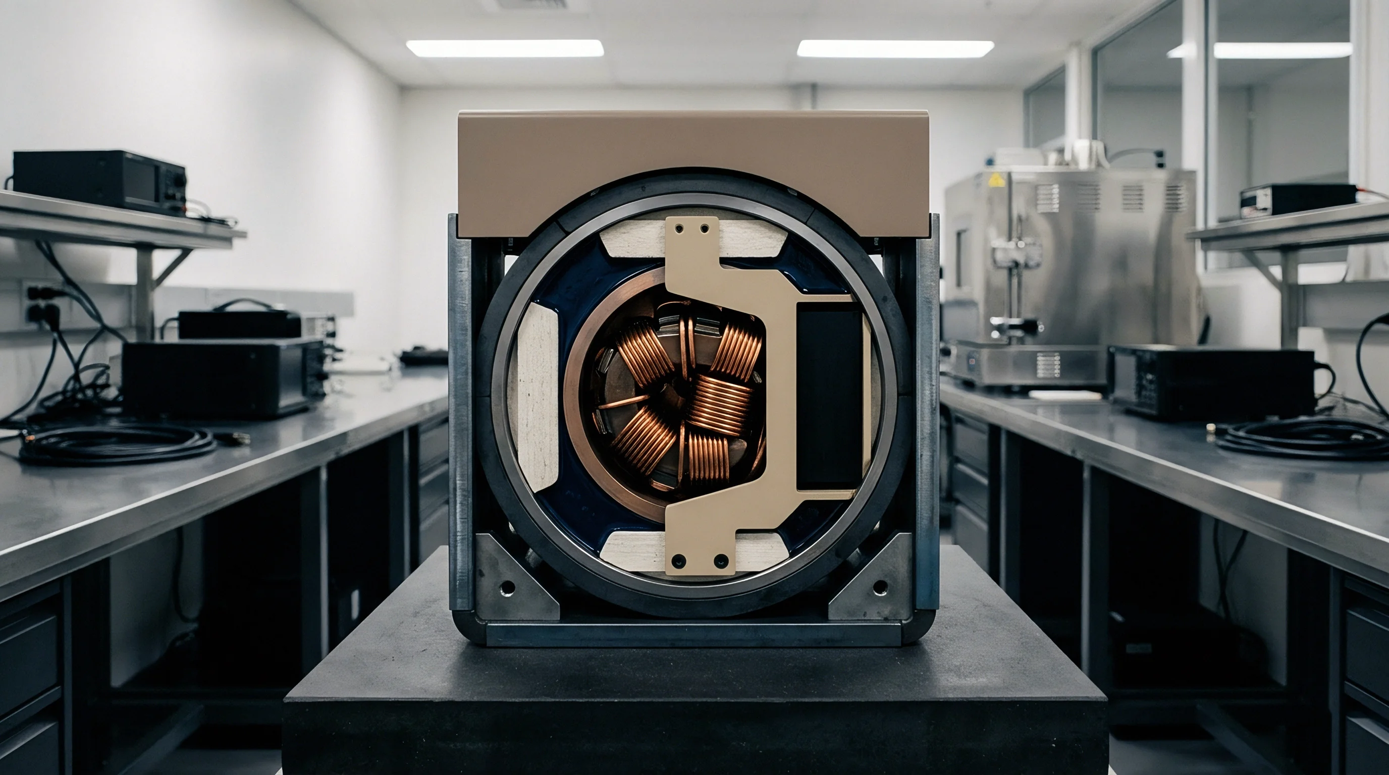
Regulatory Thresholds across International Markets
Spurious radiated limit curves defined by global regulators set mandatory compliance boundaries for multi-transmitter products. In the United States, FCC Part 15 Subpart B sets unintentional radiator field strength limits at 40.0 dBuV/m for 30 MHz to 88 MHz, 43.5 dBuV/m for 88 MHz to 216 MHz, 46.0 dBuV/m for 216 MHz to 960 MHz, and 54.0 dBuV/m for frequencies above 960 MHz at a 3-meter test distance. In Europe, ETSI EN 301 489-1 and EN 55032 mandate comparable quasi-peak and average limits, while enforcing additional radiated immunity and transient performance criteria under the Radio Equipment Directive (RED 2014/53/EU).
Asian regulatory regimes enforce stringent market-specific type approval filings and test procedures. Japan’s Giteki mark (Radio Law Article 38) and MIC regulations demand specific host-level spurious emission testing, rejecting test data generated outside accredited mutual recognition agreement (MRA) laboratories. South Korea’s National Radio Research Agency (RRA) enforces KC certification under the Radio Waves Act, requiring localized testing for host devices containing multi-radio modules.
China’s State Radio Regulatory Commission (SRRC) enforces strict fundamental power and out-of-band spurious limits, requiring certified sample submissions to in-country testing laboratories prior to commercial import authorization.
| Regulatory Region / Mark | Governing Standard | Frequency Range | Quasi-Peak Limit (3m) | Host Test Requirement |
|---|---|---|---|---|
| United States (FCC) | FCC Part 15 Class B / Part 15C | 30 MHz to 1000 MHz 1 GHz to 40 GHz | 40.0 to 46.0 dBuV/m 54.0 dBuV/m (Average) | Mandatory verification of host with all modules active |
| European Union (CE) | ETSI EN 301 489-1 / EN 55032 | 30 MHz to 1000 MHz 1 GHz to 6 GHz | 30.0 to 37.0 dBuV/m (10m) 54.0 dBuV/m (Average, 3m) | Declaration of Conformity under RED 2014/53/EU |
| Japan (Giteki) | MIC Radio Law Article 38-24 | 30 MHz to 1000 MHz 1 GHz to 26 GHz | Matches CISPR 32 Class B thresholds | Host construction compliance check + test report |
| South Korea (KC) | RRA Notice No. 2023-24 (KS X 3124) | 30 MHz to 1000 MHz 1 GHz to 6 GHz | Matches CISPR 32 Class B thresholds | In-country testing required for complete host assembly |
- Host Integration Test Report detailing radiated spurious emissions measurements with all co-located transceivers operating simultaneously at maximum rated RF power.
- Attestation Letter of Modular Conditions confirming strict adherence to all antenna gain, spatial separation, and power reduction limits specified in module grant certificates.
- Detailed Mechanical Aperture Drawings showing dimensions of all enclosure seams, display cutouts, connector interfaces, and internal shielding enclosure layouts.
- Permissive Change Class Assessment documented technical justification establishing whether host modifications qualify under Class I or Class II filing requirements.
Pre-compliance verification data, accredited chamber test reports, and accurate mechanical documentation consolidate into the final compliance dossier required to secure international market access for multi-transmitter host devices.